


 The Marketing Minute: Cracking the Code of Technical Marketing
 Trouble in Your Tank: Implementing Direct Metallization in Advanced Substrate Packaging


Researchers Produce Functional OLED Electrodes from Graphene
January 18, 2017 | Fraunhofer-GesellschaftEstimated reading time: 2 minutes
For the first time, it has been possible to produce functional OLED electrodes from graphene. The process was developed by Fraunhofer researchers together with partners from industry and research. The OLEDs can, for example, be integrated into touch displays, and the miracle material graphene promises many other applications for the future.
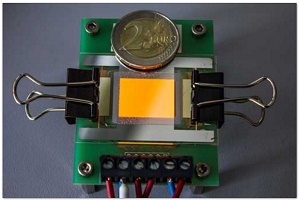
Orange luminous OLED on a graphene electrode. The two-euro coin serves as a comparison of sizes. (Image: Fraunhofer FEP)
The Fraunhofer Institute for Organic Electronics, Electron Beam and Plasma Technology FEP from Dresden, together with partners, has succeeded for the first time in producing OLED electrodes from graphene. The electrodes have an area of 2 × 1 square centimeters.
"This was a real breakthrough in research and integration of extremely demanding materials," says FEP’s project leader Dr. Beatrice Beyer.
The process was developed and optimized in the EU-funded project "Gladiator" (Graphene Layers: Production, Characterization and Integration) together with partners from industry and research.
Graphene is considered a new miracle material. The advantages of the carbon compound are impressive: graphene is light, transparent and extremely hard and has more tensile strength than steel. Moreover, it is flexible and extremely conductive for heat or electricity. Graphene consists of a single layer of carbon atoms which are assembled in a kind of honeycomb pattern. It is only 0.3 nanometers thick, which is about one hundred thousandth of a human hair. Graphene has a variety of applications – for example, as a touchscreen in smartphones.
Chemical reaction of copper, methane and hydrogen
The production of the OLED electrodes takes place in a vacuum. In a steel chamber, a wafer plate of high-purity copper is heated to about 800 degrees. The research team then supplies a mixture of methane and hydrogen and initiates a chemical reaction. The methane dissolves in the copper and forms carbon atoms, which spread on the surface. This process only takes a few minutes. After a cooling phase, a carrier polymer is placed on the graphene and the copper plate is etched away.
Gladiator project was launched in November 2013. The Fraunhofer team is working on the next steps until the conclusion in April 2017. During the remainder of the project, impurities and defects which occur during the transfer of the wafer-thin graphene to another carrier material are to be minimized. The project is supported by the EU Commission with a total of 12.4 million euros. The Fraunhofer Institute’s important industrial partners are the Spanish company Graphenea S.A., which is responsible for the production of the graphene electrodes, as well as the British Aixtron Ltd., which is responsible for the construction of the production CVD reactors.
Applications from photovoltaics to medicine
"The first products could already be launched in two to three years", says Beyer with confidence.
Due to their flexibility, the graphene electrodes are ideal for touch screens. They do not break when the device drops to the ground. Instead of glass, one would use a transparent polymer film. Many other applications are also conceivable: in windows, the transparent graphene could regulate the light transmission or serve as an electrode in polarization filters.
Graphene can also be used in photovoltaics, high-tech textiles and even in medicine.
Share on:


Testimonial
"Advertising in PCB007 Magazine has been a great way to showcase our bare board testers to the right audience. The I-Connect007 team makes the process smooth and professional. We’re proud to be featured in such a trusted publication."
Klaus Koziol - atgSuggested Items
Trouble in Your Tank: Implementing Direct Metallization in Advanced Substrate Packaging
09/15/2025 | Michael Carano -- Column: Trouble in Your TankDirect metallization systems based on conductive graphite are gaining popularity throughout the world. The environmental and productivity gains achievable with this process are outstanding. Direct metallization reduces the costs of compliance, waste treatment, and legal issues related to chemical exposure. A graphite-based direct plate system has been devised to address these needs.
Closing the Loop on PCB Etching Waste
09/09/2025 | Shawn Stone, IECAs the PCB industry continues its push toward greener, more cost-efficient operations, Sigma Engineering’s Mecer System offers a comprehensive solution to two of the industry’s most persistent pain points: etchant consumption and rinse water waste. Designed as a modular, fully automated platform, the Mecer System regenerates spent copper etchants—both alkaline and acidic—and simultaneously recycles rinse water, transforming a traditionally linear chemical process into a closed-loop system.
Driving Innovation: Depth Routing Processes—Achieving Unparalleled Precision in Complex PCBs
09/08/2025 | Kurt Palmer -- Column: Driving InnovationIn PCB manufacturing, the demand for increasingly complex and miniaturized designs continually pushes the boundaries of traditional fabrication methods, including depth routing. Success in these applications demands not only on robust machinery but also sophisticated control functions. PCB manufacturers rely on advanced machine features and process methodologies to meet their precise depth routing goals. Here, I’ll explore some crucial functions that empower manufacturers to master complex depth routing challenges.
Trouble in Your Tank: Minimizing Small-via Defects for High-reliability PCBs
08/27/2025 | Michael Carano -- Column: Trouble in Your TankTo quote the comedian Stephen Wright, “If at first you don’t succeed, then skydiving is not for you.” That can be the battle cry when you find that only small-diameter vias are exhibiting voids. Why are small holes more prone to voids than larger vias when processed through electroless copper? There are several reasons.
The Government Circuit: Navigating New Trade Headwinds and New Partnerships
08/25/2025 | Chris Mitchell -- Column: The Government CircuitAs global trade winds continue to howl, the electronics manufacturing industry finds itself at a critical juncture. After months of warnings, the U.S. Government has implemented a broad array of tariff increases, with fresh duties hitting copper-based products, semiconductors, and imports from many nations. On the positive side, tentative trade agreements with Europe, China, Japan, and other nations are providing at least some clarity and counterbalance.