


 The Marketing Minute: Cracking the Code of Technical Marketing
 Trouble in Your Tank: Implementing Direct Metallization in Advanced Substrate Packaging


Polycrystalline Materials in Solar Cells Gain New Impulse With Findings From INL Researchers
January 30, 2017 | INLEstimated reading time: 1 minute
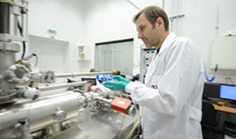
The conversion of sunlight into electricity through solar cells is considered to be a future cornerstone in a renewable energy supply for a sustainable society. The semiconducting compound Cu(In,Ga)Se2, which is deposited as a thin polycrystalline layer onto a metallized glass carrier, has long been known as an excellent light absorber. In the last 5 years, the power conversion efficiency of solar cells based on this material has reached new record values, from ~19.8% in 2011 to 22.6% in 2016, within reach of those of the commercially dominating silicon wafer technology. These recent advances have been achieved through the introduction of a potassium-fluoride treatment of the Cu(In,Ga)Se2 material. It is generally assumed that this treatment mainly affects the region of and near the charge-separating interface.
Researchers of the International Iberian Nanotechnology Laboratory (INL) in Braga have now demonstrated that also the electronic properties of the grain boundaries between the grains of the light absorbing layer are beneficially affected by the potassium treatment.
The study was performed in collaboration with researchers from the Institut des Matériaux Jean Rouxel (IMN) from the University of Nantes, who fabricated the solar cell samples and was published today in Scientific Reports, Effect of the KF post-deposition treatment on grain boundary properties in Cu(In, Ga)Se2 thin films an open access journal published by the Nature Group.
The researchers used an advanced scanning probe microscopy method to image electronic surface properties with nanometer-scale spatial resolution. “We were able to show that the potassium treatment results in a stronger and more homogeneous electronic effect at the grain boundaries” says Nicoleta Nicoara, member of the Laboratory of Nanostructured Solar Cells at INL involved in the research. Polycrystalline semiconductor materials can usually be fabricated more cost-efficient at lower processing temperatures compared to single-crystalline materials. However, the presence of grain boundaries limits their use in many applications, as they lead to losses in performance due to the presence of defects. Sascha Sadewasser who led this study summarizes: “Our study demonstrates that the potassium fluoride treatment can beneficially modify the properties of grain boundaries in Cu(In,Ga)Se2 solar cell materials. The insight we gained through our study might well influence research directions in other polycrystalline materials, and animate researcher to search for treatments with similarly positive effects on the electronic properties of grain boundaries”.
Share on:


Testimonial
"In a year when every marketing dollar mattered, I chose to keep I-Connect007 in our 2025 plan. Their commitment to high-quality, insightful content aligns with Koh Young’s values and helps readers navigate a changing industry. "
Brent Fischthal - Koh YoungSuggested Items
Curing and Verification in PCB Shadow Areas
09/17/2025 | Doug Katze, DymaxDesign engineers know a simple truth that often complicates electronics manufacturing: Light doesn’t go around corners. In densely populated PCBs, adhesives and coatings often fail to fully cure in shadowed regions created by tall ICs, connectors, relays, and tight housings.
Marcy’s Musings: Advancing the Advanced Materials Discussion
09/17/2025 | Marcy LaRont -- Column: Marcy's MusingsAs the industry’s most trusted global source of original content about the electronics supply chain, we continually ask you about your concerns, what you care about, and what you most want to learn about. Your responses are insightful and valuable. Thank you for caring enough to provide useful feedback and engage in dialogue.
September 2025 PCB007 Magazine: The Future of Advanced Materials
09/16/2025 | I-Connect007 Editorial TeamMoore’s Law is no more, and the advanced material solutions being developed to grapple with this reality are surprising, stunning, and perhaps a bit daunting. Buckle up for a dive into advanced materials and a glimpse into the next chapters of electronics manufacturing.
I-Connect007 Launches Advanced Electronics Packaging Digest
09/15/2025 | I-Connect007I-Connect007 is pleased to announce the launch of Advanced Electronics Packaging Digest (AEPD), a new monthly digital newsletter dedicated to one of the most critical and rapidly evolving areas of electronics manufacturing: advanced packaging at the interconnect level.
Panasonic Industry will Double the Production Capacity of MEGTRON Multi-layer Circuit Board Materials Over the Next Five Years
09/15/2025 | Panasonic Industry Co., Ltd.Panasonic Industry Co., Ltd., a Panasonic Group company, announced plans for a major expansion of its global production capacity for MEGTRON multi-layer circuit board materials today. The company plans to double its production over the next five years to meet growing demand in the AI server and ICT infrastructure markets.