


 Global PCB Connections: Rigid-flex and Flexible PCBs—The Backbone of Modern Electronics
 Flexible Thinking: The Key to a Successful Flex Circuit Design Transfer
 Happy’s Tech Talk #29: Bend-to-Install Semi-flex FR-4


Ventec International Expands USA Manufacturing Capacity With Investment in New Equipment
January 30, 2017 | VentecEstimated reading time: 1 minute
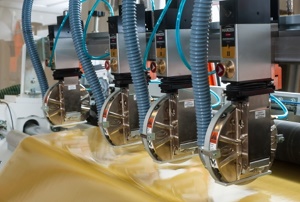
Ventec International Group has increased the manufacturing capacity at its Chicago facility (700 Lee Street, Elk Grove Village, IL) with major investment into new state-of-the-art equipment for laminate/prepregs as well as its newest ranges of PCB base-materials including complementary products such as flex and rigid-flex circuit board materials, back-up, entry and routing materials, foils and coatings.
To capture growth opportunities in prepreg markets, which are driven by particular demand from high reliability, military and aerospace applications, a Pasquato TE 15 prepreg slitter/sheeter from Italy has been installed. At the same time, cooler storage capacity has been doubled and provides ‘storage 1’ conditions of below 5oC for prepreg materials. Prepreg vacuum sealing capacity has also been doubled with the addition of a dedicated vacuum packer.
For cut-to-size back-up and entry materials, further cutting capacity is provided through the addition of a Kitagawa diamond blade saw alongside the existing Yow Shi diamond blade saw for laminate. Two Excellon Mark V Driller/Router Machines - one for tooling prepreg and one for tooling back-up and entry - have been added alongside the existing Excellon IV drill machine, adding drilling capacity to allow for materials to be supplied with tooling holes where required. Having two saws, additional drilling capability, a new shrink wrap packaging machine dedicated to packaging back-up and entry materials as well as a second delivery vehicle all in one location, offers customers a unique advantage through fast turn-around and quick-delivery material sourcing.
Jack Pattie, President of Ventec's US operation commented, "Ventec is continuing its phased and strategic investment plan across our global network of service centers. This latest investment in our Chicago facility enables our US customers to enjoy one single quick-turn access point to an extraordinary portfolio of prepregs and complementary products & services today."
About Ventec International
With volume manufacturing facilities and HQ in Suzhou China, Ventec International specializes in advanced copper clad glass reinforced and metal backed substrates for the PCB industry. With distribution locations and quick-turn CCL manufacturing sites in both the US and Europe, Ventec International is a premier supplier to the Global PCB industry. For more information, click here.
Share on:


Testimonial
"We’re proud to call I-Connect007 a trusted partner. Their innovative approach and industry insight made our podcast collaboration a success by connecting us with the right audience and delivering real results."
Julia McCaffrey - NCAB GroupSuggested Items
Closing the Loop on PCB Etching Waste
09/09/2025 | Shawn Stone, IECAs the PCB industry continues its push toward greener, more cost-efficient operations, Sigma Engineering’s Mecer System offers a comprehensive solution to two of the industry’s most persistent pain points: etchant consumption and rinse water waste. Designed as a modular, fully automated platform, the Mecer System regenerates spent copper etchants—both alkaline and acidic—and simultaneously recycles rinse water, transforming a traditionally linear chemical process into a closed-loop system.
Driving Innovation: Depth Routing Processes—Achieving Unparalleled Precision in Complex PCBs
09/08/2025 | Kurt Palmer -- Column: Driving InnovationIn PCB manufacturing, the demand for increasingly complex and miniaturized designs continually pushes the boundaries of traditional fabrication methods, including depth routing. Success in these applications demands not only on robust machinery but also sophisticated control functions. PCB manufacturers rely on advanced machine features and process methodologies to meet their precise depth routing goals. Here, I’ll explore some crucial functions that empower manufacturers to master complex depth routing challenges.
Trouble in Your Tank: Minimizing Small-via Defects for High-reliability PCBs
08/27/2025 | Michael Carano -- Column: Trouble in Your TankTo quote the comedian Stephen Wright, “If at first you don’t succeed, then skydiving is not for you.” That can be the battle cry when you find that only small-diameter vias are exhibiting voids. Why are small holes more prone to voids than larger vias when processed through electroless copper? There are several reasons.
The Government Circuit: Navigating New Trade Headwinds and New Partnerships
08/25/2025 | Chris Mitchell -- Column: The Government CircuitAs global trade winds continue to howl, the electronics manufacturing industry finds itself at a critical juncture. After months of warnings, the U.S. Government has implemented a broad array of tariff increases, with fresh duties hitting copper-based products, semiconductors, and imports from many nations. On the positive side, tentative trade agreements with Europe, China, Japan, and other nations are providing at least some clarity and counterbalance.
How Good Design Enables Sustainable PCBs
08/21/2025 | Gerry Partida, Summit InterconnectSustainability has become a key focus for PCB companies seeking to reduce waste, conserve energy, and optimize resources. While many discussions on sustainability center around materials or energy-efficient processes, PCB design is an often overlooked factor that lies at the heart of manufacturing. Good design practices, especially those based on established IPC standards, play a central role in enabling sustainable PCB production. By ensuring designs are manufacturable and reliable, engineers can significantly reduce the environmental impact of their products.