


 The Marketing Minute: Cracking the Code of Technical Marketing
 Trouble in Your Tank: Implementing Direct Metallization in Advanced Substrate Packaging


Absorbing Electromagnetic Energy While Avoiding the Heat
January 30, 2017 | Duke UniversityEstimated reading time: 2 minutes
Electrical engineers at Duke University have created the world's first electromagnetic metamaterial made without any metal. The device's ability to absorb electromagnetic energy without heating up has direct applications in imaging, sensing and lighting.
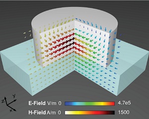
A closer look at one of the cylinders comprising a new non-metal metamaterial. The arrows depict how different aspects of an electromagnetic field interact with the cylinder.
Metamaterials are synthetic materials composed of many individual, engineered features that together produce properties not found in nature. Imagine an electromagnetic wave moving through a flat surface made of thousands of tiny electrical cells. If researchers can tune each cell to manipulate the wave in a specific way, they can dictate exactly how the wave behaves as a whole.
For researchers to manipulate electromagnetic waves, however, they've typically had to use electrically conducting metals. That approach, however, brings with it a fundamental problem of metals—the higher the electrical conductivity, the better the material also conducts heat. This limits their usefulness in temperature-dependent applications.
In a new paper, electrical engineers at Duke University demonstrate the first completely dielectric (non-metal) electromagnetic metamaterial—a surface dimpled with cylinders like the face of a Lego brick that is designed to absorb terahertz waves. While this specific frequency range sits between infrared waves and microwaves, the approach should be applicable for almost any frequency of the electromagnetic spectrum.
The results appeared online on Jan. 9 in the journal Optics Express.
"People have created these types of devices before, but previous attempts with dielectrics have always been paired with at least some metal," said Willie Padilla, professor of electrical and computer engineering at Duke University. "We still need to optimize the technology, but the path forward to several applications is much easier than with metal-based approaches."
Padilla and his colleagues created their metamaterial with boron-doped silicon—a non-metal. Using computer simulations, they calculated how terahertz waves would interact with cylinders of varying heights and widths.
The researchers then manufactured a prototype consisting of hundreds of these optimized cylinders aligned in rows on a flat surface. Physical tests showed that the new "metasurface" absorbed 97.5 percent of the energy produced by waves at 1.011 terahertz.
Efficiently absorbing energy from electromagnetic waves is an important property for many applications. For example, thermal imaging devices can operate in the terahertz range, but because they have previously included at least some metal, getting sharp images has been challenging.
"Heat propagates fast in metals, which is problematic for thermal imagers," said Xinyu Liu, a doctoral student in Padilla's laboratory and first author of the paper. "There are tricks to isolate the metal during fabrication, but that becomes cumbersome and costly."
Another potential application for the new technology is efficient lighting. Incandescent light bulbs make light but also create a significant amount of wasted heat. They must operate at high temperatures to produce light—much higher than the melting point of most metals.
"We can produce a dielectric metasurface designed to emit light, without producing waste heat," Padilla said. "Although we've already been able to do this with metal-based metamaterials, you need to operate at high temperature for the whole thing to work. Dielectric materials have melting points much higher than metals, and we're now quickly trying to move this technology into the infrared to demonstrate a lighting system."
Share on:


Testimonial
"We’re proud to call I-Connect007 a trusted partner. Their innovative approach and industry insight made our podcast collaboration a success by connecting us with the right audience and delivering real results."
Julia McCaffrey - NCAB GroupSuggested Items
Driving Innovation: Depth Routing Processes—Achieving Unparalleled Precision in Complex PCBs
09/08/2025 | Kurt Palmer -- Column: Driving InnovationIn PCB manufacturing, the demand for increasingly complex and miniaturized designs continually pushes the boundaries of traditional fabrication methods, including depth routing. Success in these applications demands not only on robust machinery but also sophisticated control functions. PCB manufacturers rely on advanced machine features and process methodologies to meet their precise depth routing goals. Here, I’ll explore some crucial functions that empower manufacturers to master complex depth routing challenges.
Polar Instruments Announces Additive Transmission Line Support for Si9000e
08/20/2025 | Polar InstrumentsTransmission lines embedded into the PCB surface are a feature of UHDI constructions. The 2025 fall release of Polar's Si9000e PCB impedance & insertion loss transmission line field solver incorporates eight new single ended, differential and coplanar transmission line structures.
Henniker Plasma Launches Stratus Turnkey Plasma Manufacturing Cell
08/13/2025 | Henniker PlasmaHenniker Plasma, a leading manufacturer of plasma treatment systems, proudly announces the launch of its Stratus Plasma Manufacturing Cell range — a fully integrated, turnkey solution that combines advanced atmospheric plasma surface treatment with robotic automation.
Trouble in Your Tank: Metallizing Flexible Circuit Materials—Mitigating Deposit Stress
08/04/2025 | Michael Carano -- Column: Trouble in Your TankMetallizing materials, such as polyimide used for flexible circuitry and high-reliability multilayer printed wiring boards, provide a significant challenge for process engineers. Conventional electroless copper systems often require pre-treatments with hazardous chemicals or have a small process window to achieve uniform coverage without blistering. It all boils down to enhancing the adhesion of the thin film of electroless copper to these smooth surfaces.
Designers Notebook: Basic PCB Planning Criteria—Establishing Design Constraints
07/22/2025 | Vern Solberg -- Column: Designer's NotebookPrinted circuit board development flows more smoothly when all critical issues are predefined and understood from the start. As a basic planning strategy, the designer must first consider the product performance criteria, then determine the specific industry standards or specifications that the product must meet. Planning also includes a review of all significant issues that may affect the product’s manufacture, performance, reliability, overall quality, and safety.