


 The Marketing Minute: Cracking the Code of Technical Marketing
 Trouble in Your Tank: Implementing Direct Metallization in Advanced Substrate Packaging


New Berkeley Lab Discovery Could Lead to Better Materials, Better Batteries
February 1, 2017 | University of California - BerkeleyEstimated reading time: 3 minutes
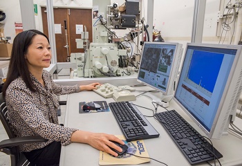
Using advanced imaging techniques, scientists at the Department of Energy’s Lawrence Berkeley National Laboratory (Berkeley Lab) have been able to observe what exactly happens inside a cathode particle as lithium-ion batteries are charged and discharged.
In a research project led by Berkeley Lab materials chemist Guoying Chen, the researchers uncovered important insights into reactions in cathode materials, including the discovery of particle cracking as the cathode is charged, which can reduce battery capacity and life. The research was published today in the journal Nature Communications in an article titled, “Phase Transformation Mechanism in LiMn1.5Ni1.5O4 Cathode Particles Revealed by Single-crystal Hard X-ray Microscopy.”
“Understanding dynamic reaction pathways in solid matter and the phase transformation mechanism is extremely difficult but critical in designing advanced materials—not just battery cathodes but materials for other applications as well,” Chen said. “The uniqueness of this work was the combination of using high-resolution two-dimensional and three-dimensional imaging techniques on single-crystal materials.”
Phase transformation—which occurs when lithium comes out of the particles as the battery is being charged or goes back in when discharged—holds the key to how fast and how many times a battery can be cycled.
For this work, Chen chose to use a lithium manganese nickel oxide cathode because it is viewed as one of the next-generation battery materials. “Its higher energy comes from its unique high charge and discharge voltage, but the high voltage also provokes enhanced reactivity from the electrolyte and leads to a less stable battery,” she said.
Using transmission microscopy imaging combined with X-ray absorption analysis, they looked at a series of samples they had prepared in the lab. “Instead of using commercial grade particles, which often have built-in variations, we made single crystals in the lab of a few microns in size,” she said. “With our samples we could carry out analysis based on observation of individual particles without worrying about contributions from other random factors not in our control, such as grain boundaries and porosity.”
The researchers mapped out the chemical and phase distribution on their particles at a very high spatial resolution. These maps provide “fossil evidence” of the phase transformation, which allowed them to achieve unprecedented mechanistic understanding of the electrode material.
What they saw was a unique nucleation and growth process involving multiple phases simultaneously on the same particle. The impact of the volume differences between the phases, a reduction of more than 6 percent in total, caused the particles to crack. This becomes more significant as the particle approaches the fully delithiated state.”
The cracking, Chen asserts, is likely one of the leading causes of the fade in long-term battery cycling that researchers have seen with this cathode. “If you have cracking, it means fresh surface keeps getting exposed, thus causing more reactions with the electrolyte, which consumes the electrolyte and reduces the lifetime of the battery,” Chen said. “If we can minimize or eliminate the cracking issue, we probably will see much improved stability.”
The researchers are examining two ideas to minimize the cracking, using smaller particles and avoiding fully charging the particles. “Reducing particle size can be tricky as it also increases the surface area,” Chen said. “Higher surface area means more side reactions to begin with, so it is important to find the optimal size.”
Meanwhile Chen said her group is also looking for other approaches for high-energy batteries, such as materials that can provide a high capacity. “The approach we developed here is broadly applicable for designing and optimizing both new and existing electrode materials,” she said.
The imaging was done at SLAC National Accelerator Laboratory’s Stanford Synchrotron Radiation Lightsource (SSRL), a Department of Energy (DOE) Office of Science User Facility. SSRL scientists Yahong Xu and Yijin Liu were co-authors of the paper, as was former Berkeley Lab postdoctoral fellow Saravanan Kuppan. The work was funded by DOE’s Energy Efficiency and Renewable Energy Office.
About Lawrence Berkeley National Laboratory
Lawrence Berkeley National Laboratory addresses the world’s most urgent scientific challenges by advancing sustainable energy, protecting human health, creating new materials, and revealing the origin and fate of the universe. Founded in 1931, Berkeley Lab’s scientific expertise has been recognized with 13 Nobel prizes. The University of California manages Berkeley Lab for the U.S. Department of Energy’s Office of Science.
Share on:


Testimonial
"The I-Connect007 team is outstanding—kind, responsive, and a true marketing partner. Their design team created fresh, eye-catching ads, and their editorial support polished our content to let our brand shine. Thank you all! "
Sweeney Ng - CEE PCBSuggested Items
Curing and Verification in PCB Shadow Areas
09/17/2025 | Doug Katze, DymaxDesign engineers know a simple truth that often complicates electronics manufacturing: Light doesn’t go around corners. In densely populated PCBs, adhesives and coatings often fail to fully cure in shadowed regions created by tall ICs, connectors, relays, and tight housings.
Marcy’s Musings: Advancing the Advanced Materials Discussion
09/17/2025 | Marcy LaRont -- Column: Marcy's MusingsAs the industry’s most trusted global source of original content about the electronics supply chain, we continually ask you about your concerns, what you care about, and what you most want to learn about. Your responses are insightful and valuable. Thank you for caring enough to provide useful feedback and engage in dialogue.
September 2025 PCB007 Magazine: The Future of Advanced Materials
09/16/2025 | I-Connect007 Editorial TeamMoore’s Law is no more, and the advanced material solutions being developed to grapple with this reality are surprising, stunning, and perhaps a bit daunting. Buckle up for a dive into advanced materials and a glimpse into the next chapters of electronics manufacturing.
I-Connect007 Launches Advanced Electronics Packaging Digest
09/15/2025 | I-Connect007I-Connect007 is pleased to announce the launch of Advanced Electronics Packaging Digest (AEPD), a new monthly digital newsletter dedicated to one of the most critical and rapidly evolving areas of electronics manufacturing: advanced packaging at the interconnect level.
Panasonic Industry will Double the Production Capacity of MEGTRON Multi-layer Circuit Board Materials Over the Next Five Years
09/15/2025 | Panasonic Industry Co., Ltd.Panasonic Industry Co., Ltd., a Panasonic Group company, announced plans for a major expansion of its global production capacity for MEGTRON multi-layer circuit board materials today. The company plans to double its production over the next five years to meet growing demand in the AI server and ICT infrastructure markets.