


 The Marketing Minute: Cracking the Code of Technical Marketing
 Trouble in Your Tank: Implementing Direct Metallization in Advanced Substrate Packaging


Thin, Flexible, Light-Absorbent Material for Energy and Stealth Applications
February 2, 2017 | UC San DiegoEstimated reading time: 3 minutes
Transparent window coatings that keep buildings and cars cool on sunny days. Devices that could more than triple solar cell efficiencies. Thin, lightweight shields that block thermal detection. These are potential applications for a thin, flexible, light-absorbing material developed by engineers at the University of California San Diego.
The material, called a near-perfect broadband absorber, absorbs more than 87 percent of near-infrared light (1,200 to 2,200 nanometer wavelengths), with 98 percent absorption at 1,550 nanometers, the wavelength for fiber optic communication. The material is capable of absorbing light from every angle. It also can theoretically be customized to absorb certain wavelengths of light while letting others pass through.
Materials that “perfectly” absorb light already exist, but they are bulky and can break when bent. They also cannot be controlled to absorb only a selected range of wavelengths, which is a disadvantage for certain applications. Imagine if a window coating used for cooling not only blocked infrared radiation, but also normal light and radio waves that transmit television and radio programs.
By developing a novel nanoparticle-based design, a team led by professors Zhaowei Liu and Donald Sirbuly at the UC San Diego Jacobs School of Engineering has created a broadband absorber that’s thin, flexible and tunable. The work was published online on Jan. 24 in Proceedings of the National Academy of Sciences.
“This material offers broadband, yet selective absorption that could be tuned to distinct parts of the electromagnetic spectrum,” Liu said.
The absorber relies on optical phenomena known as surface plasmon resonances, which are collective movements of free electrons that occur on the surface of metal nanoparticles upon interaction with certain wavelengths of light. Metal nanoparticles can carry a lot of free electrons, so they exhibit strong surface plasmon resonance — but mainly in visible light, not in the infrared.
UC San Diego engineers reasoned that if they could change the number of free electron carriers, they could tune the material’s surface plasmon resonance to different wavelengths of light. “Make this number lower, and we can push the plasmon resonance to the infrared. Make the number higher, with more electrons, and we can push the plasmon resonance to the ultraviolet region,” Sirbuly said. The problem with this approach is that it is difficult to do in metals.
To address this challenge, engineers designed and built an absorber from materials that could be modified, or doped, to carry a different amount of free electrons: semiconductors. Researchers used a semiconductor called zinc oxide, which has a moderate number of free electrons, and combined it with its metallic version, aluminum-doped zinc oxide, which houses a high number of free electrons — not as much as an actual metal, but enough to give it plasmonic properties in the infrared.
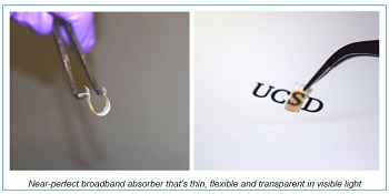
The materials were combined and structured in a precise fashion using advanced nanofabrication technologies in the Nano3 cleanroom facility at the Qualcomm Institute at UC San Diego. The materials were deposited one atomic layer at a time on a silicon substrate to create an array of standing nanotubes, each made of alternating concentric rings of zinc oxide and aluminum-doped zinc oxide. The tubes are 1,730 nanometers tall, 650 to 770 nanometers in diameter, and spaced less than a hundred nanometers apart. The nanotube array was then transferred from the silicon substrate to a thin, elastic polymer. The result is a material that is thin, flexible and transparent in the visible.
“There are different parameters that we can alter in this design to tailor the material’s absorption band: the gap size between tubes, the ratio of the materials, the types of materials, and the electron carrier concentration. Our simulations show that this is possible,” said Conor Riley, a recent nanoengineering Ph.D. graduate from UC San Diego and the first author of this work. Riley is currently a postdoctoral researcher in Sirbuly’s group.
Those are just a few exciting features of this particle-based design, researchers said. It’s also potentially transferrable to any type of substrate and can be scaled up to make large surface area devices, like broadband absorbers for large windows. “Nanomaterials normally aren’t fabricated at scales larger than a couple centimeters, so this would be a big step in that direction,” Sirbuly said.
The technology is still at the developmental stage. Liu and Sirbuly’s teams are continuing to work together to explore different materials, geometries and designs to develop absorbers that work at different wavelengths of light for various applications.
Share on:


Testimonial
"In a year when every marketing dollar mattered, I chose to keep I-Connect007 in our 2025 plan. Their commitment to high-quality, insightful content aligns with Koh Young’s values and helps readers navigate a changing industry. "
Brent Fischthal - Koh YoungSuggested Items
Curing and Verification in PCB Shadow Areas
09/17/2025 | Doug Katze, DymaxDesign engineers know a simple truth that often complicates electronics manufacturing: Light doesn’t go around corners. In densely populated PCBs, adhesives and coatings often fail to fully cure in shadowed regions created by tall ICs, connectors, relays, and tight housings.
Marcy’s Musings: Advancing the Advanced Materials Discussion
09/17/2025 | Marcy LaRont -- Column: Marcy's MusingsAs the industry’s most trusted global source of original content about the electronics supply chain, we continually ask you about your concerns, what you care about, and what you most want to learn about. Your responses are insightful and valuable. Thank you for caring enough to provide useful feedback and engage in dialogue.
September 2025 PCB007 Magazine: The Future of Advanced Materials
09/16/2025 | I-Connect007 Editorial TeamMoore’s Law is no more, and the advanced material solutions being developed to grapple with this reality are surprising, stunning, and perhaps a bit daunting. Buckle up for a dive into advanced materials and a glimpse into the next chapters of electronics manufacturing.
I-Connect007 Launches Advanced Electronics Packaging Digest
09/15/2025 | I-Connect007I-Connect007 is pleased to announce the launch of Advanced Electronics Packaging Digest (AEPD), a new monthly digital newsletter dedicated to one of the most critical and rapidly evolving areas of electronics manufacturing: advanced packaging at the interconnect level.
Panasonic Industry will Double the Production Capacity of MEGTRON Multi-layer Circuit Board Materials Over the Next Five Years
09/15/2025 | Panasonic Industry Co., Ltd.Panasonic Industry Co., Ltd., a Panasonic Group company, announced plans for a major expansion of its global production capacity for MEGTRON multi-layer circuit board materials today. The company plans to double its production over the next five years to meet growing demand in the AI server and ICT infrastructure markets.