


 The Marketing Minute: Cracking the Code of Technical Marketing
 Trouble in Your Tank: Implementing Direct Metallization in Advanced Substrate Packaging


Penn Researchers Are Among the First to Grow a Versatile Two-dimensional Material
February 8, 2017 | University of PennsylvaniaEstimated reading time: 4 minutes
University of Pennsylvania researchers are now among the first to produce a single, three-atom-thick layer of a unique two-dimensional material called tungsten ditelluride. Their findings have been published in 2-D Materials.
Unlike other two-dimensional materials, scientists believe tungsten ditelluride has what are called topological electronic states. This means that it can have many different properties not just one.
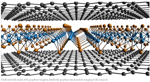
When one thinks about two-dimensional materials, graphene is probably the first that comes to mind.
The tightly packed, atomically thin sheet of carbon first produced in 2004 has inspired countless avenues in research that could revolutionize everything from technology to drinking water.
One of the most important properties of graphene is that it’s what’s called a zero bandgap semiconductor in that it can behave as both a metal and a semiconductor.
But there are tons of other properties that 2-D materials can have. Some can insulate, others can emit light and still others can be spintronic, meaning they have magnetic properties.
“Graphene is just graphene,” said A.T. Charlie Johnson, a physics professor in Penn’s School of Arts & Sciences. “It just does what graphene does. If you want to have functioning systems that are based on 2-D materials, then you want 2-D materials that have all of the different physical properties that we know about.”
The ability of 2-D materials to have topological electronic states is a phenomenon that was pioneered by Charles Kane, the Christopher H. Browne Distinguished Professor of Physics at Penn.
In this new research, Johnson, physics professor James Kikkawa and graduate students Carl Naylor and William Parkin were able to produce and measure the properties of a single layer of tungsten ditelluride.
“Because tungsten ditelluride is three atoms thick, the atoms can be arranged in different ways,” Johnson said. “These three atoms can take on slightly different configurations with respect to each other. One configuration is predicted to give these topological properties.”
Marija Drndić, the Fay R. and Eugene L. Langberg Professor of Physics; Andrew Rappe, the Blanchard Professor of Chemistry and a professor of materials science and engineering in the School of Engineering and Applied Science, and Robert Carpick, the John Henry Towne Professor and chair of the Department of Mechanical Engineering and Applied Mechanics, also contributed to the research.
“It’s very much a Penn product,” Johnson said. “We’re collaborating with multiple other faculty members who investigate the material in their own ways, and we brought it all together to put a paper out there. Everybody comes along for the ride.”
The researchers were able to grow this material using a process called chemical vapor deposition. Using a hot-tube furnace, they heated a chip containing tungsten to the right temperature and then introduced a vapor containing tellurium.
“Through good fortune and finding exactly the right conditions, these elements will chemically react and combine to form a monolayer, or three-atom-thick regions of this material,” Johnson said.
Although this material degrades extremely rapidly in air, Naylor, the paper’s first author, figured out ways to protect the material so that it could be studied before it was destroyed.
One thing the researchers found is that the material grows in little rectangular crystallites, rather than the triangles that other materials grow in.
“This reflects the rectangular symmetry in the material,” Johnson said. “They have a different structure so they tend to grow in different shapes.”
Although the research is still in its beginning stages and the researchers haven’t yet been able to produce a continuous film, they hope to conduct experiments to show that it has the topological electronic properties that are predicted.
One property of these topological systems is that any current traveling through the material would only be carried on the edges, and no current would travel through the center of the material. If researchers were able to produce single-layer-thick materials with this property, they may be able to route an electrical signal to go off into different locations.
The ability of this material to have multiple properties could also have implications in quantum computing, which taps into the power of atoms and subatomic phenomena to perform calculations significantly faster than current computers. These 2-D materials might allow for an intrinsically error-tolerant form of quantum computing called topologically protected quantum computing, which requires both semiconducting and superconducting materials.
“With these 2-D materials, you want to realize as many physical properties as possible,” Johnson said. “Topological electronic states are interesting and they're new and so a lot of people have been trying to realize them in a 2-D material. We created the material where these are predicted to occur, so in that sense we've moved towards this very big goal in the field.”
The work was supported by grants from the National Science Foundation, National Institute of Health and federal Department of Energy.
Share on:


Testimonial
"We’re proud to call I-Connect007 a trusted partner. Their innovative approach and industry insight made our podcast collaboration a success by connecting us with the right audience and delivering real results."
Julia McCaffrey - NCAB GroupSuggested Items
Curing and Verification in PCB Shadow Areas
09/17/2025 | Doug Katze, DymaxDesign engineers know a simple truth that often complicates electronics manufacturing: Light doesn’t go around corners. In densely populated PCBs, adhesives and coatings often fail to fully cure in shadowed regions created by tall ICs, connectors, relays, and tight housings.
Marcy’s Musings: Advancing the Advanced Materials Discussion
09/17/2025 | Marcy LaRont -- Column: Marcy's MusingsAs the industry’s most trusted global source of original content about the electronics supply chain, we continually ask you about your concerns, what you care about, and what you most want to learn about. Your responses are insightful and valuable. Thank you for caring enough to provide useful feedback and engage in dialogue.
September 2025 PCB007 Magazine: The Future of Advanced Materials
09/16/2025 | I-Connect007 Editorial TeamMoore’s Law is no more, and the advanced material solutions being developed to grapple with this reality are surprising, stunning, and perhaps a bit daunting. Buckle up for a dive into advanced materials and a glimpse into the next chapters of electronics manufacturing.
I-Connect007 Launches Advanced Electronics Packaging Digest
09/15/2025 | I-Connect007I-Connect007 is pleased to announce the launch of Advanced Electronics Packaging Digest (AEPD), a new monthly digital newsletter dedicated to one of the most critical and rapidly evolving areas of electronics manufacturing: advanced packaging at the interconnect level.
Panasonic Industry will Double the Production Capacity of MEGTRON Multi-layer Circuit Board Materials Over the Next Five Years
09/15/2025 | Panasonic Industry Co., Ltd.Panasonic Industry Co., Ltd., a Panasonic Group company, announced plans for a major expansion of its global production capacity for MEGTRON multi-layer circuit board materials today. The company plans to double its production over the next five years to meet growing demand in the AI server and ICT infrastructure markets.