


 The Marketing Minute: Cracking the Code of Technical Marketing
 Trouble in Your Tank: Implementing Direct Metallization in Advanced Substrate Packaging


'Editing' New Metamaterials Brings Light Into Focus
February 14, 2017 | University of California - BerkeleyEstimated reading time: 3 minutes
As cell phones have become smaller, so have their camera lenses. Phones thinner than a cut deck of cards now capture images so sharp that they can be blown up beyond movie-poster size.
When arrayed in nano-scale thin sheets, a familiar compound can be selectively heated to transform part of it into a metal yet leave the remainder transparent, an innovation that provides a range of potential applications. Photo: Peg Skorpinski
But the camera’s convex lenses impose an inherent limit on how thin the phone can be. With more than a billion-plus cell phones bought last year, manufacturers faced an unwelcome choice: either make a thicker camera or sacrifice the quality of the photos.
Now, another type of lens may be emerging, one with light-focusing power that does away with the classic convex piece of glass or plastic. Instead, it relies on “metamaterials” — fabricated arrays of nano-structures so named because they perform unlike any other natural substances.
Metamaterials are made of millions of nano-scale particles, each about the size of a virus. Although the particles themselves are made of atoms, their novel effects on material’s performance have earned them the name “artificial atoms.”
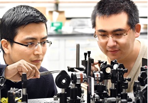
Materials scientist Jie Yao is developing a technique to fabricate one such metamaterial into a new form with strong commercial potential. He can transform a natural phase change material in a way that seems like alchemy, turning some sections of the material into metal but leaving others unchanged.
The metallic portions can interact with light as if they were nanoscale antennas, and Yao has shown that in certain conformations, the combined effect of tens of thousands of these antennas can focus light like a lens.
With support from the Bakar Fellows Program, his lab in the materials science and engineering department is fabricating nano-thin sheets of phase change material. The material is glass-like at room temperature but becomes metallic when heated slightly. Using a local heat source, Yao is able to convert part of the thin sheets into the metal antennas while letting other parts remain transparent.
The interactions of the nano-antennas with light are so effective that films hundreds of times thinner than a conventional lens could tightly control the path of light that passes through the film, Yao says.
He intends to refine his technology’s novel ability to tweak the metallic components’ 3-D shape, and he hopes to open up a range of applications to control visible light as well as infrared and microwave wavelengths.
“The metallic phase change material is the working part of the material, while the insulating part provides the matrix to hold the ‘artificial atoms’ in place,” Yao says.
“When a broad beam of light hits the array, it can be considered as composed of many finer beams. Each new beam passes by an antenna, which is able to change its unique path.
“Using a local heat source, we can ‘write’ new structures into the material. Then, by lowering the temperature, we can erase and re-write them. We can change the material’s structure, and performance at will. No complicated nano-fabrication process is needed.”
By using this etch-a-sketch local heating strategy, his team can change the material’s configuration in real time — potentially in less than a second. “In this we may be able to create a dynamic optical device, for example, a single lens whose focus can be changed whenever necessary,” Yao says.
The array can be “written” in such a way that each antenna will guide light to the same focal point to form a lens. The next moment, the array can be erased and a new array may be written, and the focal point changed to another location, which could be used to improve the performance of photography and other imaging processes.
Beyond the vision of new lenses for a billion cell phones, the technology’s ability to control visible light could yield-thin computer or wall displays. In principle, Yao says, the material and the transforming technique can yield conformations to manipulate infrared light, or microwave radiation as well, leading to novel types of infrared sensors and other optical devices.
“The material is a platform that allows us to draw any photonic structure, so we really can achieve a range of applications and transform them from static devices to dynamic ones.”
Share on:


Testimonial
"Advertising in PCB007 Magazine has been a great way to showcase our bare board testers to the right audience. The I-Connect007 team makes the process smooth and professional. We’re proud to be featured in such a trusted publication."
Klaus Koziol - atgSuggested Items
Curing and Verification in PCB Shadow Areas
09/17/2025 | Doug Katze, DymaxDesign engineers know a simple truth that often complicates electronics manufacturing: Light doesn’t go around corners. In densely populated PCBs, adhesives and coatings often fail to fully cure in shadowed regions created by tall ICs, connectors, relays, and tight housings.
Marcy’s Musings: Advancing the Advanced Materials Discussion
09/17/2025 | Marcy LaRont -- Column: Marcy's MusingsAs the industry’s most trusted global source of original content about the electronics supply chain, we continually ask you about your concerns, what you care about, and what you most want to learn about. Your responses are insightful and valuable. Thank you for caring enough to provide useful feedback and engage in dialogue.
September 2025 PCB007 Magazine: The Future of Advanced Materials
09/16/2025 | I-Connect007 Editorial TeamMoore’s Law is no more, and the advanced material solutions being developed to grapple with this reality are surprising, stunning, and perhaps a bit daunting. Buckle up for a dive into advanced materials and a glimpse into the next chapters of electronics manufacturing.
I-Connect007 Launches Advanced Electronics Packaging Digest
09/15/2025 | I-Connect007I-Connect007 is pleased to announce the launch of Advanced Electronics Packaging Digest (AEPD), a new monthly digital newsletter dedicated to one of the most critical and rapidly evolving areas of electronics manufacturing: advanced packaging at the interconnect level.
Panasonic Industry will Double the Production Capacity of MEGTRON Multi-layer Circuit Board Materials Over the Next Five Years
09/15/2025 | Panasonic Industry Co., Ltd.Panasonic Industry Co., Ltd., a Panasonic Group company, announced plans for a major expansion of its global production capacity for MEGTRON multi-layer circuit board materials today. The company plans to double its production over the next five years to meet growing demand in the AI server and ICT infrastructure markets.