


 The Marketing Minute: Cracking the Code of Technical Marketing
 Trouble in Your Tank: Implementing Direct Metallization in Advanced Substrate Packaging


NASA and MIT Collaborate to Develop Space-Based Quantum-Dot Spectrometer
February 15, 2017 | NASAEstimated reading time: 3 minutes
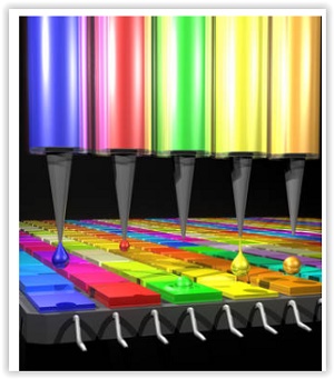
A NASA technologist has teamed with the inventor of a new nanotechnology that could transform the way space scientists build spectrometers, the all-important device used by virtually all scientific disciplines to measure the properties of light emanating from astronomical objects, including Earth itself.
Mahmooda Sultana, a research engineer at NASA’s Goddard Space Flight Center in Greenbelt, Maryland, now is collaborating with Moungi Bawendi, a chemistry professor at the Cambridge-based Massachusetts Institute of Technology, or MIT, to develop a prototype imaging spectrometer based on the emerging quantum-dot technology that Bawendi’s group pioneered.
NASA’s Center Innovation Fund, which supports potentially trailblazing, high-risk technologies, is funding the effort.
Introducing Quantum Dots
Quantum dots are a type of semiconductor nanocrystal discovered in the early 1980s. Invisible to the naked eye, the dots have proven in testing to absorb different wavelengths of light depending on their size, shape, and chemical composition. The technology is promising to applications that rely on the analysis of light, including smartphone cameras, medical devices, and environmental-testing equipment.
“This is as novel as it gets,” Sultana said, referring to the technology that she believes could miniaturize and potentially revolutionize space-based spectrometers, particularly those used on uninhabited aerial vehicles and small satellites. “It really could simplify instrument integration.”
Absorption spectrometers, as their name implies, measure the absorption of light as a function of frequency or wavelength due to its interaction with a sample, such as atmospheric gases.
After passing through or interacting with the sample, the light reaches the spectrometer. Traditional spectrometers use gratings, prisms, or interference filters to split the light into its component wavelengths, which their detector pixels then detect to produce spectra. The more intense the absorption in the spectra, the greater the presence of a specific chemical.
While space-based spectrometers are getting smaller due to miniaturization, they still are relatively large, Sultana said. “Higher-spectral resolution requires long optical paths for instruments that use gratings and prisms. This often results in large instruments. Whereas here, with quantum dots that act like filters that absorb different wavelengths depending on their size and shape, we can make an ultra-compact instrument. In other words, you could eliminate optical parts, like gratings, prisms, and interference filters.”
Just as important, the technology allows the instrument developer to generate nearly an unlimited number of different dots. As their size decreases, the wavelength of the light that the quantum dots will absorb decreases. “This makes it possible to produce a continuously tunable, yet distinct, set of absorptive filters where each pixel is made of a quantum dot of a specific size, shape, or composition. We would have precise control over what each dot absorbs. We could literally customize the instrument to observe many different bands with high-spectral resolution.”
Prototype Instrument Under Development
With her NASA technology-development support, Sultana is working to develop, qualify through thermal vacuum and vibration tests, and demonstrate a 20-by-20 quantum-dot array sensitive to visible wavelengths needed to image the sun and the aurora. However, the technology easily can be expanded to cover a broader range of wavelengths, from ultraviolet to mid-infrared, which may find many potential space applications in Earth science, heliophysics, and planetary science, she said.
Under the collaboration, Sultana is developing an instrument concept particularly for a CubeSat application and MIT doctoral student Jason Yoo is investigating techniques for synthesizing different precursor chemicals to create the dots and then printing them onto a suitable substrate. “Ultimately, we would want to print the dots directly onto the detector pixels,” she said.
“This is a very innovative technology,” Sultana added, conceding that it is very early in its development. “But we’re trying to raise its technology-readiness level very quickly. Several space-science opportunities that could benefit are in the pipeline.”
Share on:


Testimonial
"We’re proud to call I-Connect007 a trusted partner. Their innovative approach and industry insight made our podcast collaboration a success by connecting us with the right audience and delivering real results."
Julia McCaffrey - NCAB GroupSuggested Items
Blaize, Technology Control Company Partner to Power Saudi Arabia’s Next-Generation AI Innovation Infrastructure
09/17/2025 | BUSINESS WIREBlaize Holdings, Inc., a leader in programmable, energy-efficient edge AI computing, and Technology Control Company (TCC), a leading technology solutions provider in the Kingdom of Saudi Arabia (KSA), announced a strategic partnership to advance Saudi Arabia’s AI innovation infrastructure and accelerate its digital transformation goals.
BLT Joins Microchip Partner Program as Design Partner
09/17/2025 | BUSINESS WIREBLT, a U.S.-owned and operated engineering design services firm announced it has joined the Microchip Design Partner Program.
Curing and Verification in PCB Shadow Areas
09/17/2025 | Doug Katze, DymaxDesign engineers know a simple truth that often complicates electronics manufacturing: Light doesn’t go around corners. In densely populated PCBs, adhesives and coatings often fail to fully cure in shadowed regions created by tall ICs, connectors, relays, and tight housings.
On the Line With… Podcast: UHDI and RF Performance
09/17/2025 | I-Connect007I-Connect007 is excited to announce the release of a new episode in its latest On the Line with... podcast series, which shines a spotlight on one of the most important emerging innovations in electronics manufacturing: Ultra-High-Density Interconnect (UHDI).
Altair, Wichita State University’s NIAR Sign MoU to Accelerate Aerospace Innovation
09/16/2025 | AltairAltair, a global leader in computational intelligence, and Wichita State University’s (WSU) National Institute for Aviation Research (NIAR), one of the world’s leading aerospace research institutions, have signed a memorandum of understanding (MoU) to advance innovation across the aerospace and defense industries.