


 The Marketing Minute: Cracking the Code of Technical Marketing
 Trouble in Your Tank: Implementing Direct Metallization in Advanced Substrate Packaging


Surprising Spin Behavior at Room Temperature
February 17, 2017 | Tokyo Institute of TechnologyEstimated reading time: 2 minutes
Surprising spin behavior at room temperature: circularly polarized room-temperature electroluminescence from spin-polarized light-emitting diodes.
Scientists at Tokyo Institute of Technology have observed almost purely circularly polarized electroluminescence from GaAs-based spin-polarized light-emitting diodes at room temperature, with no external magnetic field. This behavior indicates the presence of spin-dependent nonlinear processes, which may allow the development of semiconductor-based spin-photonic devices in the future.
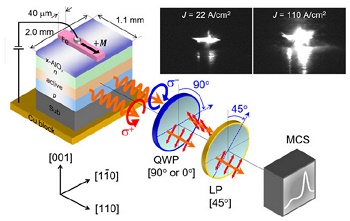
Figure 1. Spin-LED chip placed on a copper block (left) and emitting CP EL (orange spiral arrows); the right- (σ+) and left (σ-)-handed EL components are indicated by the red and blue circles, respectively. QWP, LP, and MCS represent a quarter-wave plate, a linear polarizer, and a multichannel spectrometer, respectively. Inset: EL from a spin-LED chip for different current densities.
The field of spintronics focuses on spin transport behavior in magnetic metals, and the major findings in this area have important implications for the field of electronics. This is because conventional electronics primarily considers the electron charge, whereas spintronics allows the electron spin to be exploited. One of the most significant advancements in spintronics has been the introduction of spin degrees of freedom to semiconductors, which are essential components of modern electronic and photonic applications. However, most experiments investigating spin manipulation in semiconductors have been performed under high magnetic fields and at cryogenic temperatures.
Recently, Specially Appointed Assistant Professor Nozomi Nishizawa and Professor Hiro Munekata and colleagues, from the Institute of Innovative Research, Tokyo Institute of Technology, examined the behavior of spin-polarized light-emitting diodes (LEDs) at room temperature and without an external magnetic field. Hence, they achieved the unexpected result of almost purely circularly polarized (CP) electroluminescence (EL).
The LEDs used in the study contained an epitaxial double heterostructure (sandwich-like structure) of AlGaAs/GaAs/AlGaAs, a crystalline γ-like AlOx tunnel barrier (for electrical stability during operation), and a polycrystalline Fe in-plane spin injector. During operation, spins of a given type were injected into the device. Spin relaxation then caused these spins to disperse and adopt other orthogonal orientations. Radiative recombination subsequently occurred, which was observed in the form of a linearly polarized emission.
Experiments on the LED chips showed that a higher current density generated an increase in the emission intensity. Nishizawa and coworkers also noted that the difference between the left- and right-handed EL components increased with the current density. Specifically, the intensity of the left-handed minority component decreased with increased current density, whereas that of the right-handed majority component increased linearly. Therefore, when the current density was sufficiently high (~100 A/cm2), almost pure CP was achieved. Investigating this behavior in more detail, the researchers found that p-type doping in the active layer allowed the CP observation, which arose from spin-dependent nonlinear processes occurring at a sufficiently high current density.
In the future, higher current densities will be applied in order to elucidate the mechanism behind these nonlinear processes and to investigate the possibility of stimulated CP emission in other geometries. Other important avenues of investigation also exist, e.g., potential spin-LED applications in secure optical communications, cancer diagnosis, and optically enhanced nuclei imaging.
Share on:


Testimonial
"The I-Connect007 team is outstanding—kind, responsive, and a true marketing partner. Their design team created fresh, eye-catching ads, and their editorial support polished our content to let our brand shine. Thank you all! "
Sweeney Ng - CEE PCBSuggested Items
Trouble in Your Tank: Implementing Direct Metallization in Advanced Substrate Packaging
09/15/2025 | Michael Carano -- Column: Trouble in Your TankDirect metallization systems based on conductive graphite are gaining popularity throughout the world. The environmental and productivity gains achievable with this process are outstanding. Direct metallization reduces the costs of compliance, waste treatment, and legal issues related to chemical exposure. A graphite-based direct plate system has been devised to address these needs.
Closing the Loop on PCB Etching Waste
09/09/2025 | Shawn Stone, IECAs the PCB industry continues its push toward greener, more cost-efficient operations, Sigma Engineering’s Mecer System offers a comprehensive solution to two of the industry’s most persistent pain points: etchant consumption and rinse water waste. Designed as a modular, fully automated platform, the Mecer System regenerates spent copper etchants—both alkaline and acidic—and simultaneously recycles rinse water, transforming a traditionally linear chemical process into a closed-loop system.
Driving Innovation: Depth Routing Processes—Achieving Unparalleled Precision in Complex PCBs
09/08/2025 | Kurt Palmer -- Column: Driving InnovationIn PCB manufacturing, the demand for increasingly complex and miniaturized designs continually pushes the boundaries of traditional fabrication methods, including depth routing. Success in these applications demands not only on robust machinery but also sophisticated control functions. PCB manufacturers rely on advanced machine features and process methodologies to meet their precise depth routing goals. Here, I’ll explore some crucial functions that empower manufacturers to master complex depth routing challenges.
Trouble in Your Tank: Minimizing Small-via Defects for High-reliability PCBs
08/27/2025 | Michael Carano -- Column: Trouble in Your TankTo quote the comedian Stephen Wright, “If at first you don’t succeed, then skydiving is not for you.” That can be the battle cry when you find that only small-diameter vias are exhibiting voids. Why are small holes more prone to voids than larger vias when processed through electroless copper? There are several reasons.
The Government Circuit: Navigating New Trade Headwinds and New Partnerships
08/25/2025 | Chris Mitchell -- Column: The Government CircuitAs global trade winds continue to howl, the electronics manufacturing industry finds itself at a critical juncture. After months of warnings, the U.S. Government has implemented a broad array of tariff increases, with fresh duties hitting copper-based products, semiconductors, and imports from many nations. On the positive side, tentative trade agreements with Europe, China, Japan, and other nations are providing at least some clarity and counterbalance.