


 The Marketing Minute: Cracking the Code of Technical Marketing
 Trouble in Your Tank: Implementing Direct Metallization in Advanced Substrate Packaging


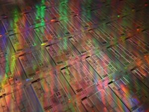
New Resource for Optical Chips
February 21, 2017 | MITEstimated reading time: 5 minutes
The Semiconductor Industry Association has estimated that at current rates of increase, computers’ energy requirements will exceed the world’s total power output by 2040.
Using light rather than electricity to move data would dramatically reduce computer chips’ energy consumption, and the past 20 years have seen remarkable progress in the development of silicon photonics, or optical devices that are made from silicon so they can easily be integrated with electronics on silicon chips.
But existing silicon-photonic devices rely on different physical mechanisms than the high-end optoelectronic components in telecommunications networks do. The telecom devices exploit so-called second-order nonlinearities, which make optical signal processing more efficient and reliable.
In the latest issue of Nature Photonics, MIT researchers present a practical way to introduce second-order nonlinearities into silicon photonics. They also report prototypes of two different silicon devices that exploit those nonlinearities: a modulator, which encodes data onto an optical beam, and a frequency doubler, a component vital to the development of lasers that can be precisely tuned to a range of different frequencies.
In optics, a linear system is one whose outputs are always at the same frequencies as its inputs. So a frequency doubler, for instance, is an inherently nonlinear device.
“We now have the ability to have a second-order nonlinearity in silicon, and this is the first real demonstration of that,” says Michael Watts, an associate professor of electrical engineering and computer science at MIT and senior author on the new paper.
“Now you can build a phase modulator that is not dependent on the free-carrier effect in silicon. The benefit there is that the free-carrier effect in silicon always has a phase and amplitude coupling. So whenever you change the carrier concentration, you’re changing both the phase and the amplitude of the wave that’s passing through it. With second-order nonlinearity, you break that coupling, so you can have a pure phase modulator. That’s important for a lot of applications. Certainly in the communications realm that’s important.”
The first author on the new paper is Erman Timurdogan, who completed his PhD at MIT last year and is now at the silicon-photonics company Analog Photonics. He and Watts are joined by Matthew Byrd, an MIT graduate student in electrical engineering and computer science, and Christopher Poulton, who did his master’s in Watts’s group and is also now at Analog Photonics.
Dopey solutions
If an electromagnetic wave can be thought of as a pattern of regular up-and-down squiggles, a digital modulator perturbs that pattern in fixed ways to represent strings of zeroes and ones. In a silicon modulator, the path that the light wave takes is defined by a waveguide, which is rather like a rail that runs along the top of the modulator.
Existing silicon modulators are doped, meaning they have had impurities added to them through a standard process used in transistor manufacturing. Some doping materials yield p-type silicon, where the “p” is for “positive,” and some yield n-type silicon, where the “n” is for “negative.” In the presence of an electric field, free carriers — electrons that are not associated with particular silicon atoms — tend to concentrate in n-type silicon and to dissipate in p-type silicon.
A conventional silicon modulator is half p-type and half n-type silicon; even the waveguide is split right down the middle. On either side of the waveguide are electrodes, and changing the voltage across the modulator alternately concentrates and dissipates free carriers in the waveguide, to modulate an optical signal passing through.
The MIT researchers’ device is similar, except that the center of the modulator — including the waveguide that runs along its top — is undoped. When a voltage is applied, the free carriers don’t collect in the center of the device; instead, they build up at the boundary between the n-type silicon and the undoped silicon. A corresponding positive charge builds up at the boundary with the p-type silicon, producing an electric field, which is what modulates the optical signal.
Because the free carriers at the center of a conventional silicon modulator can absorb light particles — or photons — traveling through the waveguide, they diminish the strength of the optical signal; modulators that exploit second-order nonlinearities don’t face that problem.
Picking up speed
In principle, they can also modulate a signal more rapidly than existing silicon modulators do. That’s because it takes more time to move free carriers into and out of the waveguide than it does to concentrate and release them at the boundaries with the undoped silicon. The current paper simply reports the phenomenon of nonlinear modulation, but Timurdogan says that the team has since tested prototypes of a modulator whose speeds are competitive with those of the nonlinear modulators found in telecom networks.
The frequency doubler that the researchers demonstrated has a similar design, except that the regions of p- and n-doped silicon that flank the central region of undoped silicon are arranged in regularly spaced bands, perpendicular to the waveguide. The distances between the bands are calibrated to a specific wavelength of light, and when a voltage is applied across them, they double the frequency of the optical signal passing through the waveguide, combining pairs of photons into single photons with twice the energy.
Frequency doublers can be used to build extraordinarily precise on-chip optical clocks, optical amplifiers, and sources of terahertz radiation, which has promising security applications.
“Silicon has had a huge renaissance within the optical communication space for a variety of applications,” says Jason Orcutt, a researcher in the Physical Sciences Department at IBM's Thomas J. Watson Research Center. “However, there are still remaining application spaces — from microwave photonics to quantum optics — where the lack of second-order nonlinear effects in silicon has prevented progress. This is an important step towards addressing a wider range of applications within the mature silicon-photonics platforms around the world.”
“To date, efforts to achieve second-order nonlinear effects in silicon have focused on hard material-science problems,” Orcutt adds. “The [MIT] team has been extremely clever by reminding the physics community what we shouldn't have forgotten. Applying a simple electric field creates the same basic crystal polarization vector that other researchers have worked hard to create by far more complicated means.”
Share on:


Testimonial
"Advertising in PCB007 Magazine has been a great way to showcase our bare board testers to the right audience. The I-Connect007 team makes the process smooth and professional. We’re proud to be featured in such a trusted publication."
Klaus Koziol - atgSuggested Items
Beyond Design: Slaying Signal Integrity Villains
09/17/2025 | Barry Olney -- Column: Beyond DesignHigh-speed PCB design is a balancing act, where subtle oversights can develop into major signal integrity nightmares. Some culprits lie dormant during early validation, only to reveal themselves later through workflow disruptions and elusive performance bottlenecks. Take crosstalk, for example. What begins as a stray signal coupling between traces can ripple through the design, ultimately destabilizing the power distribution network. Each of these troublemakers operates with signature tactics, but they also have well-known vulnerabilities.
Staying on Top of Signal Integrity Challenges
09/16/2025 | Andy Shaughnessy, Design007 MagazineOver the years, Kris Moyer has taught a variety of advanced PCB design classes, both online IPC courses and in-person classes at California State University-Sacramento, where he earned his degrees in electrical engineering. Much of his advanced curriculum focuses on signal integrity, so we asked Kris to discuss the trends he’s seeing in signal integrity today, the SI challenges facing PCB designers, and his go-to techniques for controlling or completely eliminating SI problems.
September 2025 PCB007 Magazine: The Future of Advanced Materials
09/16/2025 | I-Connect007 Editorial TeamMoore’s Law is no more, and the advanced material solutions being developed to grapple with this reality are surprising, stunning, and perhaps a bit daunting. Buckle up for a dive into advanced materials and a glimpse into the next chapters of electronics manufacturing.
Elementary Mr. Watson: Running the Signal Gauntlet
09/11/2025 | John Watson -- Column: Elementary, Mr. WatsonIf you’ve ever run a military obstacle course, you know it’s less “fun fitness challenge” and more “how can we inflict as much pain in the shortest time possible?” You start fresh—chest out, lungs full of confidence, thinking you might even look good doing this—and 10 seconds later, you’re questioning all your life choices.
The Shaughnessy Report: Winning the Signal Integrity Battle
09/09/2025 | Andy Shaughnessy -- Column: The Shaughnessy ReportWhen I first started covering this industry in 1999, signal integrity was the hip new thing in PCB design. Conference classes on signal integrity were packed to the walls, and an SI article was guaranteed to get a lot of reads.