


 The Marketing Minute: Cracking the Code of Technical Marketing
 Trouble in Your Tank: Implementing Direct Metallization in Advanced Substrate Packaging


Machine Learning Helps Researchers Design Less Costly Optical Sensors
February 21, 2017 | UCLAEstimated reading time: 3 minutes
Finding practical solutions to detect proteins, cancer biomarkers, viruses and other small objects has been a key challenge for researchers worldwide for decades. These solutions hold promise for saving lives through more timely diagnosis and treatment of serious infections and diseases.
Now a UCLA team’s new research shows how such detections might be done for a fraction of the cost by using “smart” mobile devices designed by machine learning.
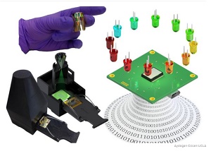
One method to detect small objects and related biomarkers is called plasmonic sensing, which involves shining light onto metal nanostructures to amplify the local electric field. The interaction between this amplified electric field and the molecule of interest can be measured, revealing important information about molecular concentration and kinetics. Although scientists have explored this type of sensing for decades, they have faced challenges when it comes to environments outside of laboratory settings that are limited in resources. This is because expensive and bulky instruments are needed for this work.
The primary goal of machine learning is to “train” an algorithm with a large amount of data so that it can “learn” complex trends and statistics and in turn be used to predict outcomes with far more accuracy than a traditional model. For example, Google has been using machine learning in such applications as recognizing letters and numbers on our streets and homes.
The UCLA team, led by Aydogan Ozcan, Chancellor’s Professor of Electrical Engineering and Bioengineering and associate director of the California NanoSystems Institute, took this concept and applied it to plasmonic sensing, constructing a mobile and inexpensive device that is far more accurate than conventional sensor designs.
The prototype device is lightweight and portable, consisting of a 3D printed plastic housing, four light-emitting diodes, or LEDs, of different colors and a camera. As described in the study, a machine learning algorithm selects the four most optimal LEDs out of thousands of other possible choices, coming up with the most accurate design, and a computational method to quantify the sensor output. This work aims to provide a design tool that other engineers and researchers can use to optimize their own low-cost optical sensor readers for various applications in health care as well as environmental monitoring.
By using newly discovered nanofabrication methods, the research team was able to produce flexible plasmonic sensors that are robust and inexpensive enough to be disposable. These sensors can undergo “surface modification,” which ensures that only the molecules of interest interact with the amplified electric field.
This biochemistry step can be thought of like two complementary puzzle pieces, where one piece is attached to the sensor surface, preventing any other piece other than its complement to join it and interfere with the measurement. This means these sensors can be “modified” to capture any number of specific bio-targets such as bacteria, viruses or cancer cells, among many others.
To use this plasmonic reader, a fluidic specimen, for example blood or urine, is applied to the sensor surface using a disposable microchip. The sensor then fits into a cartridge that can be inserted into the device, which then automatically measures and analyzes the specimen, delivering the sensing result. The research team says that such a plasmonic reader could be designed as a mobile-phone attachment to further drive down the costs and take advantage of cloud connectivity as well as the computational power of smartphones.
“Amazing discoveries and results are being made daily at research institutions like UCLA, but oftentimes when engineers begin to envision moving this science into the real world, they hit roadblocks,” Ballard said. “So it is always exciting to me to see cutting-edge technology become more practical.”
The research was supported by the National Science Foundation, the National Institutes of Health, the Office of Naval Research, the Army Research Office, and the Howard Hughes Medical Institute.
Share on:


Testimonial
"The I-Connect007 team is outstanding—kind, responsive, and a true marketing partner. Their design team created fresh, eye-catching ads, and their editorial support polished our content to let our brand shine. Thank you all! "
Sweeney Ng - CEE PCBSuggested Items
Meet the Author Podcast: Martyn Gaudion Unpacks the Secrets of High-Speed PCB Design
07/16/2025 | I-Connect007In this special Meet the Author episode of the On the Line with… podcast, Nolan Johnson sits down with Martyn Gaudion, signal integrity expert, managing director of Polar Instruments, and three-time author in I-Connect007’s popular The Printed Circuit Designer’s Guide to... series.
Intervala Hosts Employee Car and Motorcycle Show, Benefit Nonprofits
08/27/2024 | IntervalaIntervala hosted an employee car and motorcycle show, aptly named the Vala-Cruise and it was a roaring success! Employees had the chance to show off their prized wheels, and it was incredible to see the variety and passion on display.
KIC Honored with IPC Recognition for 25 Years of Membership and Contributions to Electronics Manufacturing Industry
06/24/2024 | KICKIC, a renowned pioneer in thermal process and temperature measurement solutions for electronics manufacturing, is proud to announce that it has been recognized by IPC for 25 years of membership and significant contributions to electronics manufacturing.
Boeing Starliner Spacecraft Completes Successful Crewed Docking with International Space Station
06/07/2024 | BoeingNASA astronauts Barry "Butch" Wilmore and Sunita "Suni" Williams successfully docked Boeing's Starliner spacecraft to the International Space Station (ISS), about 26 hours after launching from Cape Canaveral Space Force Station.
KIC’s Miles Moreau to Present Profiling Basics and Best Practices at SMTA Wisconsin Chapter PCBA Profile Workshop
01/25/2024 | KICKIC, a renowned pioneer in thermal process and temperature measurement solutions for electronics manufacturing, announces that Miles Moreau, General Manager, will be a featured speaker at the SMTA Wisconsin Chapter In-Person PCBA Profile Workshop.