


 The Marketing Minute: Cracking the Code of Technical Marketing
 Trouble in Your Tank: Implementing Direct Metallization in Advanced Substrate Packaging


Researchers Pave the Way for Ionotronic Nanodevices
February 23, 2017 | Aalto UniversityEstimated reading time: 2 minutes
Ionotronic devices rely on charge effects based on ions, instead of electrons or in addition to electrons. These devices open new opportunities for creating electrically switchable memories. However, there are still many technical challenges to overcome before this new kind of memories can be produced.
Researchers at Aalto University in Finland have visualized how oxygen ion migration in a complex oxide material causes the material to alter its crystal structure in a uniform and reversible fashion, prompting large modulations of electrical resistance. They performed simultaneous imaging and resistance measurements in a transmission electron microscope using a sample holder with a nanoscale electrical probe. Resistance-switching random access memories could utilize this effect.
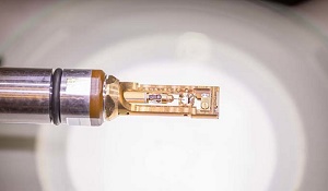
Sample holder helps control of migration of ions
“In a transmission electron microscope, a beam of high-energy electrons is transmitted through a very thin specimen. Various detectors collect the electrons after their interaction with the sample, providing detailed information about the atomic structure and composition of the material. The technique is extremely powerful for nanomaterials characterization, but if used conventionally, it does not allow for active material manipulation inside the microscope. In our study, we utilized a special sample holder with a piezo-controlled metallic probe to make an electrical nanocontact. This in situ method allowed us to apply short voltage pulses and thereby control the migration of oxygen ions in our sample,” explains Academy of Finland Research Fellow Lide Yao from the Department of Applied Physics.
The researchers found that migration of oxygen ions away from the contact area results in an abrupt change in the oxide lattice structure and an increase of electrical resistance. Reversal of the voltage polarity fully restores the original material properties. Electro-thermal simulations, performed by PhD candidate Sampo Inkinen, showed that a combination of current-induced sample heating and electric-field-directed ion migration causes the switching effect.
Ionotronic concept can be applied for manipulation of several material properties
“The material that we investigated in this study is a complex oxide. Complex oxides can exhibit many interesting physical properties including magnetism, ferroelectricity, and superconductivity, and all these properties vary sensitively with the oxidation state of the material. Voltage-induced migration of oxygen ions does change the amount of oxidation, triggering strong material responses. While we have demonstrated direct correlations between oxygen content, crystal structure, and electrical resistance, the same ionotronic concept could be utilized to control other material properties,” says Professor Sebastiaan van Dijken, who is a coauthor on the paper.
Academy of Finland Research Fellow Lide Yao and the research group performed the study at Aalto University’s Nanomicroscopy Center for high-resolution material characterization and part of Finland’s national research infrastructure, OtaNano. Photo Mikko Raskinen.
“In the current study, we employed a special sample holder for simultaneous measurements of the atomic-scale structure and electrical resistance. We are now developing an entirely new and unique holder that would allow for transmission electron microscopy measurements while the specimen is irradiated by intense light. We plan to investigate atomic scale processes in perovskite solar cells and other optoelectronic materials with this setup in the future,” adds Yao.
Share on:


Testimonial
"The I-Connect007 team is outstanding—kind, responsive, and a true marketing partner. Their design team created fresh, eye-catching ads, and their editorial support polished our content to let our brand shine. Thank you all! "
Sweeney Ng - CEE PCBSuggested Items
MEMS & Imaging Sensors Summit to Spotlight Sensing Revolution for Europe’s Leadership
09/11/2025 | SEMIIndustry experts will gather November 19-20 at the SEMI MEMS & Imaging Sensors Summit 2025 to explore the latest breakthroughs in AI-driven MEMS and imaging optimization, AR/VR technologies, and advanced sensor solutions for critical defence applications.
Direct Imaging System Market Size to Hit $4.30B by 2032, Driven by Increasing Demand for High-Precision PCB Manufacturing
09/11/2025 | Globe NewswireAccording to the SNS Insider, “The Direct Imaging System Market size was valued at $2.21 Billion in 2024 and is projected to reach $4.30 Billion by 2032, growing at a CAGR of 8.68% during 2025-2032.”
I-Connect007’s Editor’s Choice: Five Must-Reads for the Week
07/04/2025 | Marcy LaRont, I-Connect007For our industry, we have seen several bullish market announcements over the past few weeks, including one this week by IDC on the massive growth in the global server market. We’re also closely watching global trade and nearshoring. One good example of successful nearshoring is Rehm Thermal Systems, which celebrates its 10th anniversary in Mexico and the official opening of its new building in Guadalajara.
Driving Innovation: Direct Imaging vs. Conventional Exposure
07/01/2025 | Simon Khesin -- Column: Driving InnovationMy first camera used Kodak film. I even experimented with developing photos in the bathroom, though I usually dropped the film off at a Kodak center and received the prints two weeks later, only to discover that some images were out of focus or poorly framed. Today, every smartphone contains a high-quality camera capable of producing stunning images instantly.
United Electronics Corporation Advances Manufacturing Capabilities with Schmoll MDI-ST Imaging Equipment
06/24/2025 | United Electronics CorporationUnited Electronics Corporation has successfully installed the advanced Schmoll MDI-ST (XL) imaging equipment at their advanced printed circuit board facility. This significant technology investment represents a continued commitment to delivering superior products and maintaining their position as an industry leader in precision PCB manufacturing.