


 The Marketing Minute: Cracking the Code of Technical Marketing
 Trouble in Your Tank: Implementing Direct Metallization in Advanced Substrate Packaging


Nanotube Growth Moving in the Right Direction
February 24, 2017 | LLNLEstimated reading time: 1 minute
For the first time, Lawrence Livermore National Laboratory scientists and collaborators have captured a movie (link is external) of how large populations of carbon nanotubes grow and align themselves.
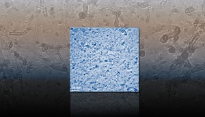
This transmission electron microscope image shows growth of a dense carbon nanotube population.
Understanding how carbon nanotubes (CNT) nucleate, grow and self-organize to form macroscale materials is critical for application-oriented design of next-generation supercapacitors, electronic interconnects, separation membranes and advanced yarns and fabrics.
New research by LLNL scientist Eric Meshot and colleagues from Brookhaven National Laboratory (link is external) (BNL) and Massachusetts Institute of Technology (link is external) (MIT) has demonstrated direct visualization of collective nucleation and self-organization of aligned carbon nanotube films inside of an environmental transmission electron microscope (ETEM).
In a pair of studies reported in recent issues of Chemistry of Materials (link is external) and ACS Nano (link is external), the researchers leveraged a state-of-the-art kilohertz camera in an aberration-correction ETEM at BNL to capture the inherently rapid processes that govern the growth of these exciting nanostructures.
Among other phenomena discovered, the researchers are the first to provide direct proof of how mechanical competition among neighboring carbon nanotubes can simultaneously promote self-alignment while also frustrating and limiting growth.
"This knowledge may enable new pathways toward mitigating self-termination and promoting growth of ultra-dense and aligned carbon nanotube materials, which would directly impact several application spaces, some of which are being pursued here at the Laboratory," Meshot said.
Meshot has led the CNT synthesis development at LLNL for several projects, including those supported by the Laboratory Directed Research and Development (LDRD) program and the Defense Threat Reduction Agency (link is external) (DTRA) that use CNTs as fluidic nanochannels for applications ranging from single-molecule detection to macroscale membranes for breathable and protective garments.
Share on:


Testimonial
"The I-Connect007 team is outstanding—kind, responsive, and a true marketing partner. Their design team created fresh, eye-catching ads, and their editorial support polished our content to let our brand shine. Thank you all! "
Sweeney Ng - CEE PCBSuggested Items
Curing and Verification in PCB Shadow Areas
09/17/2025 | Doug Katze, DymaxDesign engineers know a simple truth that often complicates electronics manufacturing: Light doesn’t go around corners. In densely populated PCBs, adhesives and coatings often fail to fully cure in shadowed regions created by tall ICs, connectors, relays, and tight housings.
Marcy’s Musings: Advancing the Advanced Materials Discussion
09/17/2025 | Marcy LaRont -- Column: Marcy's MusingsAs the industry’s most trusted global source of original content about the electronics supply chain, we continually ask you about your concerns, what you care about, and what you most want to learn about. Your responses are insightful and valuable. Thank you for caring enough to provide useful feedback and engage in dialogue.
September 2025 PCB007 Magazine: The Future of Advanced Materials
09/16/2025 | I-Connect007 Editorial TeamMoore’s Law is no more, and the advanced material solutions being developed to grapple with this reality are surprising, stunning, and perhaps a bit daunting. Buckle up for a dive into advanced materials and a glimpse into the next chapters of electronics manufacturing.
I-Connect007 Launches Advanced Electronics Packaging Digest
09/15/2025 | I-Connect007I-Connect007 is pleased to announce the launch of Advanced Electronics Packaging Digest (AEPD), a new monthly digital newsletter dedicated to one of the most critical and rapidly evolving areas of electronics manufacturing: advanced packaging at the interconnect level.
Panasonic Industry will Double the Production Capacity of MEGTRON Multi-layer Circuit Board Materials Over the Next Five Years
09/15/2025 | Panasonic Industry Co., Ltd.Panasonic Industry Co., Ltd., a Panasonic Group company, announced plans for a major expansion of its global production capacity for MEGTRON multi-layer circuit board materials today. The company plans to double its production over the next five years to meet growing demand in the AI server and ICT infrastructure markets.