


 The Marketing Minute: Cracking the Code of Technical Marketing
 Trouble in Your Tank: Implementing Direct Metallization in Advanced Substrate Packaging


Nano ‘Sandwich’ Offers Unique Properties
February 28, 2017 | Rice UniversityEstimated reading time: 2 minutes
Rice University researchers have modeled a nanoscale sandwich, the first in what they hope will become a molecular deli for materials scientists.
Their recipe puts two slices of atom-thick graphene around nanoclusters of magnesium oxide that give the super-strong, conductive material expanded optoelectronic properties.
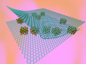
Nanoclusters of magnesium oxide sandwiched between layers of graphene make a compound with unique electronic and optical properties, according to researchers at Rice University who made computer simulations of the material.
Nanoclusters of magnesium oxide sandwiched between layers of graphene make a compound with unique electronic and optical properties, according to researchers at Rice University who made computer simulations of the material. Illustration by Lei Tao
Rice materials scientist Rouzbeh Shahsavari and his colleagues built computer simulations of the compound and found it would offer features suitable for sensitive molecular sensing, catalysis and bio-imaging. Their work could help researchers design a range of customizable hybrids of two- and three-dimensional structures with encapsulated molecules, Shahsavari said.
The scientists were inspired by experiments elsewhere in which various molecules were encapsulated using van der Waals forces to draw components together. The Rice-led study was the first to take a theoretical approach to defining the electronic and optical properties of one of those “made” samples, two-dimensional magnesium oxide in bilayer graphene, Shahsavari said.
“We knew if there was an experiment already performed, we would have a great reference point that would make it easier to verify our computations, thus allowing more reliable expansion of our computational results to identify performance trends beyond the reach of experiments,” Shahsavari said.
Graphene on its own has no band gap – the characteristic that makes a material a semiconductor. But the hybrid does, and this band gap could be tunable, depending on the components, Shahsavari said. The enhanced optical properties are also tunable and useful, he said.
“We saw that while this single flake of magnesium oxide absorbed one kind of light emission, when it was trapped between two layers of graphene, it absorbed a wide spectrum. That could be an important mechanism for sensors,” he said.
Shahsavari said his group’s theory should be applicable to other two-dimensional materials, like hexagonal boron-nitride, and molecular fillings. “There is no single material that can solve all the technical problems of the world,” he said. “It always comes down to making hybrid materials to synergize the best features of multiple components to do a specific job. My group is working on these hybrid materials by tweaking their components and structures to meet new challenges.”
Farzaneh Shayeganfar, a visiting research scientist at Rice and researcher at Shahid Rajaee Teacher Training University, Tehran, Iran, is lead author of the paper. Co-authors are Javad Beheshtiyan and Mehdi Neek-Amal, both of Shahid Rajaee and the University of Antwerp, Belgium.
Rice University and the Iran Science Elites Federation supported the research. Computing resources were supplied by Rice’s National Science Foundation-supported DAVinCI supercomputer administered by Rice’s Center for Research Computing and were procured in partnership with Rice’s Ken Kennedy Institute for Information Technology.
Share on:


Testimonial
"In a year when every marketing dollar mattered, I chose to keep I-Connect007 in our 2025 plan. Their commitment to high-quality, insightful content aligns with Koh Young’s values and helps readers navigate a changing industry. "
Brent Fischthal - Koh YoungSuggested Items
Curing and Verification in PCB Shadow Areas
09/17/2025 | Doug Katze, DymaxDesign engineers know a simple truth that often complicates electronics manufacturing: Light doesn’t go around corners. In densely populated PCBs, adhesives and coatings often fail to fully cure in shadowed regions created by tall ICs, connectors, relays, and tight housings.
Marcy’s Musings: Advancing the Advanced Materials Discussion
09/17/2025 | Marcy LaRont -- Column: Marcy's MusingsAs the industry’s most trusted global source of original content about the electronics supply chain, we continually ask you about your concerns, what you care about, and what you most want to learn about. Your responses are insightful and valuable. Thank you for caring enough to provide useful feedback and engage in dialogue.
September 2025 PCB007 Magazine: The Future of Advanced Materials
09/16/2025 | I-Connect007 Editorial TeamMoore’s Law is no more, and the advanced material solutions being developed to grapple with this reality are surprising, stunning, and perhaps a bit daunting. Buckle up for a dive into advanced materials and a glimpse into the next chapters of electronics manufacturing.
I-Connect007 Launches Advanced Electronics Packaging Digest
09/15/2025 | I-Connect007I-Connect007 is pleased to announce the launch of Advanced Electronics Packaging Digest (AEPD), a new monthly digital newsletter dedicated to one of the most critical and rapidly evolving areas of electronics manufacturing: advanced packaging at the interconnect level.
Panasonic Industry will Double the Production Capacity of MEGTRON Multi-layer Circuit Board Materials Over the Next Five Years
09/15/2025 | Panasonic Industry Co., Ltd.Panasonic Industry Co., Ltd., a Panasonic Group company, announced plans for a major expansion of its global production capacity for MEGTRON multi-layer circuit board materials today. The company plans to double its production over the next five years to meet growing demand in the AI server and ICT infrastructure markets.