


 The Marketing Minute: Cracking the Code of Technical Marketing
 Trouble in Your Tank: Implementing Direct Metallization in Advanced Substrate Packaging


Imprinting Technology Improves Transistor-Based Biosensors
February 28, 2017 | ACN NewswireEstimated reading time: 1 minute
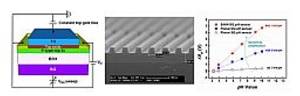
Korean researchers are improving the fabrication of transistor-based biosensors by using silicon nanowires on their surface. The team, led by Won-Ju Cho of Kwangwoon University in Seoul, based their device on the 'dual-gate field-effect transistor' (DG FET).
When molecules bind on a field-effect transistor, a change happens in the surface's electric charge. This makes FETs good candidates for detecting biological and chemical elements. Dual-gate FETs are particularly good candidates because they amplify this signal several times. But they can still be improved.
The team used a method called 'nanoimprint lithography' to fabricate silicon nanowires onto the surface of a DG FET and compared its sensitivity and stability with conventional DG FETs.
Field-effect transistors using silicon nanowires have already been drawing attention as promising biosensors because of their high sensitivity and selectivity, but they are difficult to manufacture. The size and position of silicon nanowires fabricated using a bottom-up approach, such as chemical vapor deposition, cannot always be perfectly controlled. Top-down approaches, such as using an electron or ion beam to draw nanorods onto a surface, allow better control of size and shape, yet they are expensive and limited by low throughput.
Cho and his colleagues fabricated their silicon nanowires using nanoimprint lithography. In this method, a thin layer of silicon was placed on top of a substrate. This layer was then pressed using a nanoimprinter, which imprints nano-sized wire-shaped lines into the surface. The areas between separate lines were then removed using a method called dry etching, which involves bombarding the material with chlorine ions. The resultant silicon nanowires were then added to a DG FET.
The team found that their device was more stable and sensitive than conventional DG FETs. "We expect that the silicon-nanowire DG FET sensor proposed here could be developed into a promising label-free sensor for various biological events, such as enzyme-substrate reactions, antigen-antibody bindings and nucleic acid hybridizations [a method used to detect gene sequences]," conclude the researchers in their study published in the journal Science and Technology of Advanced Materials.
Share on:


Testimonial
"We’re proud to call I-Connect007 a trusted partner. Their innovative approach and industry insight made our podcast collaboration a success by connecting us with the right audience and delivering real results."
Julia McCaffrey - NCAB GroupSuggested Items
Driving Innovation: Depth Routing Processes—Achieving Unparalleled Precision in Complex PCBs
09/08/2025 | Kurt Palmer -- Column: Driving InnovationIn PCB manufacturing, the demand for increasingly complex and miniaturized designs continually pushes the boundaries of traditional fabrication methods, including depth routing. Success in these applications demands not only on robust machinery but also sophisticated control functions. PCB manufacturers rely on advanced machine features and process methodologies to meet their precise depth routing goals. Here, I’ll explore some crucial functions that empower manufacturers to master complex depth routing challenges.
Polar Instruments Announces Additive Transmission Line Support for Si9000e
08/20/2025 | Polar InstrumentsTransmission lines embedded into the PCB surface are a feature of UHDI constructions. The 2025 fall release of Polar's Si9000e PCB impedance & insertion loss transmission line field solver incorporates eight new single ended, differential and coplanar transmission line structures.
Henniker Plasma Launches Stratus Turnkey Plasma Manufacturing Cell
08/13/2025 | Henniker PlasmaHenniker Plasma, a leading manufacturer of plasma treatment systems, proudly announces the launch of its Stratus Plasma Manufacturing Cell range — a fully integrated, turnkey solution that combines advanced atmospheric plasma surface treatment with robotic automation.
Trouble in Your Tank: Metallizing Flexible Circuit Materials—Mitigating Deposit Stress
08/04/2025 | Michael Carano -- Column: Trouble in Your TankMetallizing materials, such as polyimide used for flexible circuitry and high-reliability multilayer printed wiring boards, provide a significant challenge for process engineers. Conventional electroless copper systems often require pre-treatments with hazardous chemicals or have a small process window to achieve uniform coverage without blistering. It all boils down to enhancing the adhesion of the thin film of electroless copper to these smooth surfaces.
Designers Notebook: Basic PCB Planning Criteria—Establishing Design Constraints
07/22/2025 | Vern Solberg -- Column: Designer's NotebookPrinted circuit board development flows more smoothly when all critical issues are predefined and understood from the start. As a basic planning strategy, the designer must first consider the product performance criteria, then determine the specific industry standards or specifications that the product must meet. Planning also includes a review of all significant issues that may affect the product’s manufacture, performance, reliability, overall quality, and safety.