


 The Marketing Minute: Cracking the Code of Technical Marketing
 Trouble in Your Tank: Implementing Direct Metallization in Advanced Substrate Packaging


Learning How to Fine-Tune Nanofabrication
March 2, 2017 | Tokyo Institute of TechnologyEstimated reading time: 2 minutes
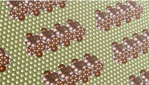
Daniel Packwood, at Kyoto University's Institute for Integrated Cell-Material Sciences (iCeMS), Patrick Han at Advanced Institute for Materials Research (AIMR), Tohoku University and Taro Hitosugi at Tokyo Institute of Technology (and Visiting Professor at AIMR, Tohoku University) are improving methods for constructing tiny "nanomaterials" using a "bottom-up" approach called "molecular self-assembly". Using this method, molecules are chosen according to their ability to spontaneously interact and combine to form shapes with specific functions. In the future, this method may be used to produce tiny wires with diameters 1/100,000th that of a piece of hair, or tiny electrical circuits that can fit on the tip of a needle.
Molecular self-assembly is a spontaneous process that cannot be controlled directly by laboratory equipment, so it must be controlled indirectly. This is done by carefully choosing the direction of the intermolecular interactions, known as "chemical control", and carefully choosing the temperature at which these interactions happen, known as "entropic control".
Researchers know that when entropic control is very weak, for example, molecules are under chemical control and assemble in the direction of the free sites available for molecule-to-molecule interaction. On the other hand, self-assembly does not occur when entropic control is much stronger than the chemical control, and the molecules remain randomly dispersed.
Until now, it's not been possible for researchers to guess what kinds of structures will result from molecular self-assembly when entropic control is neither weak nor strong compared to chemical control.
Packwood teamed up with colleagues in Japan and the U.S. to develop a computational method that allows them to simulate molecular self-assembly on metal surfaces while separating the effects of chemical and entropic controls.
This new computational method makes use of artificial intelligence to simulate how molecules behave when placed on a metal surface. Specifically, a "machine learning" technique is used to analyse a database of intermolecular interactions. This machine learning technique builds a model that encodes the information contained in the database, and in turn this model can predict the outcome of the molecular self-assembly process with high accuracy.
The team used this method to study the self-assembly of three different hydrocarbon molecules, the structures of which vary in the strength of the direction of their intermolecular interactions. In other words, they varied the strength of chemical control by changing the molecule under study.
While stronger chemical control caused molecules to assemble into chain-shaped structures, the effects of stronger entropic controls were found to be more counterintuitive. For example, they found that strengthening entropic control could transform large, disordered structures into several small, ordered, chain-shaped structures. They also showed that the formation of disordered structures results from weak chemical control rather than strong entropic control.
These predictions, which were verified by comparisons with high-resolution microscopic images of real molecules on metal surfaces, may lead to controlled, large-scale fabrication of tiny electrical wires and other nanomaterials for future devices. Devices made from nanomaterials would be significantly smaller and cheaper than existing electronics, and would have very long battery lives due to low energy consumption.
"By continued development of our code and theory, we expect to obtain increasingly detailed rules for controlling molecular self-assembly and aiding the bottom-up nanomaterials fabrication process," the researchers conclude in their study published in the journal Nature Communications.
Share on:


Testimonial
"In a year when every marketing dollar mattered, I chose to keep I-Connect007 in our 2025 plan. Their commitment to high-quality, insightful content aligns with Koh Young’s values and helps readers navigate a changing industry. "
Brent Fischthal - Koh YoungSuggested Items
Trouble in Your Tank: Implementing Direct Metallization in Advanced Substrate Packaging
09/15/2025 | Michael Carano -- Column: Trouble in Your TankDirect metallization systems based on conductive graphite are gaining popularity throughout the world. The environmental and productivity gains achievable with this process are outstanding. Direct metallization reduces the costs of compliance, waste treatment, and legal issues related to chemical exposure. A graphite-based direct plate system has been devised to address these needs.
Closing the Loop on PCB Etching Waste
09/09/2025 | Shawn Stone, IECAs the PCB industry continues its push toward greener, more cost-efficient operations, Sigma Engineering’s Mecer System offers a comprehensive solution to two of the industry’s most persistent pain points: etchant consumption and rinse water waste. Designed as a modular, fully automated platform, the Mecer System regenerates spent copper etchants—both alkaline and acidic—and simultaneously recycles rinse water, transforming a traditionally linear chemical process into a closed-loop system.
Driving Innovation: Depth Routing Processes—Achieving Unparalleled Precision in Complex PCBs
09/08/2025 | Kurt Palmer -- Column: Driving InnovationIn PCB manufacturing, the demand for increasingly complex and miniaturized designs continually pushes the boundaries of traditional fabrication methods, including depth routing. Success in these applications demands not only on robust machinery but also sophisticated control functions. PCB manufacturers rely on advanced machine features and process methodologies to meet their precise depth routing goals. Here, I’ll explore some crucial functions that empower manufacturers to master complex depth routing challenges.
Trouble in Your Tank: Minimizing Small-via Defects for High-reliability PCBs
08/27/2025 | Michael Carano -- Column: Trouble in Your TankTo quote the comedian Stephen Wright, “If at first you don’t succeed, then skydiving is not for you.” That can be the battle cry when you find that only small-diameter vias are exhibiting voids. Why are small holes more prone to voids than larger vias when processed through electroless copper? There are several reasons.
The Government Circuit: Navigating New Trade Headwinds and New Partnerships
08/25/2025 | Chris Mitchell -- Column: The Government CircuitAs global trade winds continue to howl, the electronics manufacturing industry finds itself at a critical juncture. After months of warnings, the U.S. Government has implemented a broad array of tariff increases, with fresh duties hitting copper-based products, semiconductors, and imports from many nations. On the positive side, tentative trade agreements with Europe, China, Japan, and other nations are providing at least some clarity and counterbalance.