


 It’s Only Common Sense: Customers Capabilities—and Confidence
 Beyond the Board: How a Diminished Supplier Base Affects Complex PCB Manufacturing Readiness in Defense


Semiconductor Photonic Nanocavities on Paper Substrates
March 2, 2017 | KAISTEstimated reading time: 2 minutes
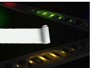
Professor Yong-Hoon Cho of the Department of Physics and his team at KAIST have developed a semiconductor photonic nanocavity laser that can operate on a paper substrate.
The method, which involves transferring nano-sized photonic crystal particles onto a paper substrate with high absorptiveness, is expected to enable the diagnosis of various diseases by using high-tech semiconductor sensors that are produced at low costs.
Photonic crystals, utilizing light as a medium to provide high bandwidths, can transfer large amounts of information. Compared with their electronic counterparts, photonic crystals consume less energy as they require less power for operation.
Normally, semiconductor photonic particles require substrates, which merely play a passive role in the assembly and endurance of individual, functional photonic components. These substrates, however, take up considerable amount of volume, and are environmentally hazardous as they are made up of non-biodegradable materials.
The research team overcame these two shortcomings by replacing a semiconductor substrate with standard paper. The substrate’s bulky size was discarded, and because paper is made from trees, it is naturally degradable. Paper can be easily and cheaply acquired in our surroundings, thereby drastically reducing the unit cost of semiconductors.
Paper also possesses superior mechanical characteristics. It is flexible and can be repeatedly folded and unfolded without being torn. These are the traits that have long been coveted by existing flexible substrates.
The research team used a micro-sized stamp to detach photonic crystal nanobeam cavities selectively from their original substrate and transfer them onto a new paper substrate. Using this technique, the team was able to remove nanophotonic crystals that had been patterned (process of selectively etching circuits onto a substrate) onto a semiconductor substrate with a high degree of integration, and realign them as desired on a paper substrate.
The nanophotonic crystals that the team combined with paper in this research are 0.5 micrometers in width, 6 micrometers in length, and 0.3 micrometers in height—about one-hundredth of the width of a single hair (0.1 millimeter).
The team also transferred their photonic crystals onto paper with a fluid channel, hence proving that it can be used as a refractive index sensor. As can be seen in pregnancy diagnosis kits that have already been commercialized, paper has high absorptiveness. Since photonic crystal particles have high sensitivity, they are highly suitable for application as sensors.
Professor Cho stated that “by using paper substrates, this technology can greatly contribute to the rising field of producing environmentally-friendly photonic particles” and “combining inexpensive paper and high-performance photonic crystal sensors allows us to attain low prices as well as designing appropriate technologies with high performance.”
Dr. Sejeong Kim of the Department of Physics participated in this study as the first author, and Professor Kwanwoo Shin of Sogang University and Professor Yong-Hee Lee of KAIST also took part in this research. The research was supported by the National Research Foundation’s Mid-Career Researcher Program, and the Climate Change Research Hub of KAIST.
Share on:


Subscribe
Stay ahead of the technologies shaping the future of electronics with our latest newsletter, Advanced Electronics Packaging Digest. Get expert insights on advanced packaging, materials, and system-level innovation, delivered straight to your inbox.Subscribe now to stay informed, competitive, and connected.
Suggested Items
AT&S Advances Glass Core Substrates for AI, HPC, and Photonics
04/22/2026 | AT&SAT&S is advancing glass core substrates from research toward industrial use in artificial intelligence, high-performance computing, high-speed communications and photonics.
IBM, UIUC Expand Discovery Accelerator for AI and Quantum Computing
04/20/2026 | PRNewswireIBM and the Grainger College of Engineering at the University of Illinois Urbana-Champaign (U. of I.) announced an expansion of the IBM-Illinois Discovery Accelerator Institute.
Long Night of Research 2026: AT&S Brings Artificial Intelligence to Life
04/15/2026 | AT&SWhen the Long Night of Research takes place throughout Austria on Friday, April 24, setting an example for the country’s innovative strength, AT&S will be there with a special highlight.
Foxconn Recognized as Top 100 Global Innovators 2026
04/14/2026 | FoxconnHon Hai Technology Group (Foxconn) has been named in Clarivate’s Top 100 Global Innovators 2026, a milestone for the ninth year running and as the accelerating role of artificial intelligence stood out in innovation activity among peers in the prestigious ranking.
Carbice Awarded Multi-Million Dollar U.S. Navy Contract for Thermal Assembly Joint Technology
04/14/2026 | PRNewswireCarbice, a U.S.-based manufacturer and supplier of novel multifunctional assembly joint technologies, has been awarded a multi-million dollar contract by the U.S. Navy's Office of Naval Research.