


 The Marketing Minute: Cracking the Code of Technical Marketing
 Trouble in Your Tank: Implementing Direct Metallization in Advanced Substrate Packaging


Towards Mastering Terahertz Waves With Graphene
March 7, 2017 | Université de GenèveEstimated reading time: 2 minutes
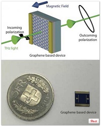
The terahertz waves span frequency ranges between the infrared spectrum (used, for example, for night vision) and gigahertz waves (which find their application, among other, in Wi-Fi connections). Terahertz waves allow for the detection of materials that are undetectable at other frequencies. However, the use of these waves is severely limited by the absence of suitable devices and materials allowing to control them.
Researchers at the University of Geneva (UNIGE), working with the Federal Polytechnic School in Zurich (ETHZ) and two Spanish research teams, have developed a technique based on the use of graphene, which allows for the potentially very quick control of both the intensity and the polarization of terahertz light. This discovery, presented in Nature Communications ("Electrically controlled terahertz magneto-optical phenomena in continuous and patterned graphene"), paves the way for a practical use of terahertz waves, in particular for imaging and telecommunications.
Graphene is a single atomic layer of carbon atoms that form a honeycomb network. It is found for example in graphite, the main constituent of pencil rods. In the Department of Quantum Matter Physics of UNIGE's Faculty of Sciences, Alexey Kuzmenko's team has been working on graphene's physical properties for several years. "The interaction between terahertz radiation and the electrons in graphene is very strong and we have therefore come to the hypothesis that it should be possible to use graphene to manage terahertz waves," Kuzmenko explains.
Working within the framework of the European project Graphene Flagship, scientists have made a graphene-based transistor adapted to terahertz waves.
"By combining the electrical field, which enables us to control the number of electrons in graphene and thus allows more or less light to pass through, with the magnetic field, which bends the electronic orbits, we have been able to control not just the intensity of the terahertz waves, but also their polarisation," comments Jean-Marie Poumirol, a member of the UNIGE research team and the first author of the study. "It is rare that purely electrical effects are used to control magnetic phenomena."
Scientists are now able to apply such control over a complete range of terahertz frequencies.
Practical applications of terahertz waves
Today, the UNIGE research team's focus is to move on from the prototype, and develop practical applications and new opportunities by controlling terahertz waves. Their objective is to make terahertz waves industrially competitive in the next few years.
There are two main areas of application for this innovation, the first being communications.
"Using a film of graphene associated with terahertz waves, we should be potentially able to send fully-secured information at speeds of about 10 to 100 times faster than with Wi-Fi or radio waves, and do it securely over short distances," explains Poumirol.
This would present a significant advantage in telecommunications. The second sphere of application is that of imaging. Being non-ionising, terahertz waves do not alter DNA and therefore are very useful in medicine, biology and pharmacy.
Additionally, the control of the circular polarization of the terahertz waves will allow distinction between different symmetries (left-handed or right-handed) of biological molecules, which is a very important property in medical applications.
Furthermore, there is potentially a very powerful application of these waves in homeland security.
Kuzmenko continues, "Terahertz waves are stopped by metals and are sensitive to plastics and organic matter. This could lead to more effective means of detecting firearms, drugs and explosives carried by individuals, and could perhaps serve as a tool to strengthen airport safety."
Share on:


Testimonial
"We’re proud to call I-Connect007 a trusted partner. Their innovative approach and industry insight made our podcast collaboration a success by connecting us with the right audience and delivering real results."
Julia McCaffrey - NCAB GroupSuggested Items
MEMS & Imaging Sensors Summit to Spotlight Sensing Revolution for Europe’s Leadership
09/11/2025 | SEMIIndustry experts will gather November 19-20 at the SEMI MEMS & Imaging Sensors Summit 2025 to explore the latest breakthroughs in AI-driven MEMS and imaging optimization, AR/VR technologies, and advanced sensor solutions for critical defence applications.
Direct Imaging System Market Size to Hit $4.30B by 2032, Driven by Increasing Demand for High-Precision PCB Manufacturing
09/11/2025 | Globe NewswireAccording to the SNS Insider, “The Direct Imaging System Market size was valued at $2.21 Billion in 2024 and is projected to reach $4.30 Billion by 2032, growing at a CAGR of 8.68% during 2025-2032.”
I-Connect007’s Editor’s Choice: Five Must-Reads for the Week
07/04/2025 | Marcy LaRont, I-Connect007For our industry, we have seen several bullish market announcements over the past few weeks, including one this week by IDC on the massive growth in the global server market. We’re also closely watching global trade and nearshoring. One good example of successful nearshoring is Rehm Thermal Systems, which celebrates its 10th anniversary in Mexico and the official opening of its new building in Guadalajara.
Driving Innovation: Direct Imaging vs. Conventional Exposure
07/01/2025 | Simon Khesin -- Column: Driving InnovationMy first camera used Kodak film. I even experimented with developing photos in the bathroom, though I usually dropped the film off at a Kodak center and received the prints two weeks later, only to discover that some images were out of focus or poorly framed. Today, every smartphone contains a high-quality camera capable of producing stunning images instantly.
United Electronics Corporation Advances Manufacturing Capabilities with Schmoll MDI-ST Imaging Equipment
06/24/2025 | United Electronics CorporationUnited Electronics Corporation has successfully installed the advanced Schmoll MDI-ST (XL) imaging equipment at their advanced printed circuit board facility. This significant technology investment represents a continued commitment to delivering superior products and maintaining their position as an industry leader in precision PCB manufacturing.