


 Dan's Biz Bookshelf: 'Getting Naked: A Business Fable'
 The Chemical Connection: Common Misconceptions in Wet Processing
 It’s Only Common Sense: Selling to Engineers


Coffee-Ring Effect Leads to Crystallization Control in Semiconductors
March 9, 2017 | KAUSTEstimated reading time: 2 minutes
A chance observation of crystals forming a mark that resembled the stain of a coffee cup left on a table has led to the growth of customized polycrystals with implications for faster and more versatile semiconductors.
Thin-film semiconductors are the foundation of a vast array of electronic and optoelectronic devices. They are generally fabricated by crystallization processes that yield polycrystals with a chaotic mix of individual crystals of different orientations and sizes.
Significant advances in controlling crystallization has been made by a team led by Professor Aram Amassian of Material Science and Engineering at KAUST. The group included individuals from the KAUST Solar Center and others from the University’s Physical Science and Engineering Division in collaboration with Cornell University. Amassian said, “There is no longer a need to settle for random and incoherent crystallization.”
The team’s recent discovery began when Dr. Liyang Yu of the KAUST team noticed that a droplet of liquid semiconductor material dried to form an outer coffee-ring shape that was much thicker than the material at the center. When he induced the material to crystallize, the outer ring crystallized first.
“This hinted that local thickness matters for initiating crystallization,” said Amassian, which went against the prevailing understanding of how polycrystal films form.
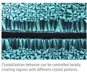
This anomaly led the researchers to delve deeper. They found that the thickness of the crystallizing film could be used to manipulate the crystallization of many materials (see top image). Most crucially, tinkering with the thickness also allowed fine control over the position and orientation of the crystals in different regions of a semiconductor.
“We discovered how to achieve excellent semiconductor properties everywhere in a polycrystal film,” said Amassian. He explained that seeding different patterns of crystallization at different locations also allowed the researchers to create bespoke arrays that can now be used in electronic circuits.
This is a huge improvement to the conventional practice of making do with materials whose good properties are not sustained throughout the entire polycrystal nor whose functions at different regions can be controlled.
“We can now make customized polycrystals on demand,” Amassian said.
Amassian hopes that this development will lead to high-quality, tailored polycrystal semiconductors to promote advances in optoelectronics, photovoltaics and printed electronic components. The method has the potential to bring more efficient consumer electronic devices, some with flexible and lightweight parts, new solar power generating systems and advances in medical electronics. And all thanks to the chance observation of an odd pattern in a semiconductor droplet.
The team will now explore ways to move their work beyond the laboratory through industry partnerships and research collaborations.
Share on:


Suggested Items
DuPont Reports First Quarter 2025 Results
05/02/2025 | PRNewswireDuPont announced its financial results for the first quarter ended March 31, 2025.
'Chill Out' with TopLine’s President Martin Hart to Discuss Cold Electronics at SPWG 2025
05/02/2025 | TopLineBraided Solder Columns can withstand the rigors of deep space cold and cryogenic environments, and represent a robust new solution to challenges facing next generation large packages in electronics assembly.
Alternative Manufacturing Inc. (AMI) Appoints Gregory Picard New Business Development Manager
05/01/2025 | Alternative Manufacturing, Inc.Alternative Manufacturing Inc. (AMI) is pleased to announce the appointment of Mr. Gregory Picard as our new Business Development Manager. Picard brings a wealth of experience in Sales and Business Development, having worked with some of the most prominent names in the industry.
Indium Wins EM Asia Innovation Award
05/01/2025 | Indium CorporationIndium Corporation, a leading materials provider for the electronics assembly market, recently earned an Electronics Manufacturing (EM) Asia Innovation Award for its new high-reliability Durafuse® HR alloy for solder paste at Productronica China in Shanghai.
Discover the Future of AI in Test and Inspection in the May 2025 Issue of SMT007 Magazine
05/01/2025 | I-Connect007 Editorial TeamAre you ready to explore the cutting-edge advancements in AI shaping the electronics manufacturing industry through test and inspection? The May 2025 issue of SMT007 Magazine provides insights, innovations, and perspectives from today's top experts you won't find anywhere else.