


 The Marketing Minute: Cracking the Code of Technical Marketing
 Trouble in Your Tank: Implementing Direct Metallization in Advanced Substrate Packaging


Perovskite Edges Can Be Tuned for Optoelectronic Performance
March 10, 2017 | Los Alamos National LaboratoryEstimated reading time: 2 minutes
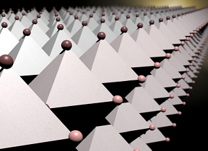
In the eternal search for next generation high-efficiency solar cells and LEDs, scientists at Los Alamos National Laboratory and their partners are creating innovative 2D layered hybrid perovskites that allow greater freedom in designing and fabricating efficient optoelectronic devices. Industrial and consumer applications could include low cost solar cells, LEDs, laser diodes, detectors, and other nano-optoelectronic devices.
“Our material is a layered compound, meaning it is a stack of 2D layers of perovskites with nanometer thickness (like a stack of sheets), and the 2D perovskite layers are separated by thin organic layers,” said Jean-Christophe Blancon, lead author on a paper out today in the journal Science’s First Release distribution. “This work could overturn conventional wisdom on the limitations of device designs based on layered perovskites.”
The 2D, near-single-crystalline “Ruddlesden-Popper” thin films have an out-of-plane orientation so that uninhibited charge transport occurs through the perovskite layers in planar devices. At the edges of the perovskite layers, the new research discovered “layer-edge-states,” which are key to both high efficiency of solar cells (>12 percent) and high fluorescence efficiency (a few tens of percent) for LEDs. The spontaneous conversion of excitons (bound electron-hole pairs) to free carriers via these layer-edge states appears to be the key to improving the photovoltaic and light-emitting thin-film layered materials.
The team investigated both photophysical and optoelectronic properties of phase-pure homogenous 2D perovskites. They were able to show that thin films have an intrinsic mechanism for dissociation of the strongly bound electron-hole pairs (excitons) to long-lived free-carriers provided by lower energy states at the edges of the layered perovskites.
Moreover, once carriers are trapped in these edge states, they remain protected and do not lose their energy via non-radiative processes. They can contribute to photocurrent in a photovoltaic (PV) device or radiatively recombine efficiently for light-emission applications. “These materials are quantum hybrid materials, possessing physical properties of both organic semiconductors and inorganic semiconducting quantum wells. We are just beginning to understand the interplay of the organic and inorganic components in 2D perovskites and this result underpins how unique properties can arise from competing physical properties,” said Jared Crochet of the Physical Chemistry and Applied Spectroscopy group at Los Alamos.
“These results address a long-standing problem not just for the perovskite family, but relevant to a large group of materials where edges and surface states generally degrade the optoelectronic properties, which can now be chemically designed and engineered to achieve efficient flow of charge and energy leading to high-efficiency optoelectronic devices,” said Aditya Mohite, who leads the perovskite program in the Material Synthesis and Integrated devices group at Los Alamos.
“The 2D hybrid perovskites continue to surprise. When we first designed these materials we were hoping that high quality samples of them would exhibit novel optoelectronic properties,” said co-author Mercouri Kanatzidis of Northwestern University. “Well, they have done so and then some. They have exceeded our expectations and are proving to be truly amazing systems. We have only scratched the surface of what is there—sorry for the pun—in this 2D family and we anticipate continued excitement going forward.”
Share on:


Testimonial
"Advertising in PCB007 Magazine has been a great way to showcase our bare board testers to the right audience. The I-Connect007 team makes the process smooth and professional. We’re proud to be featured in such a trusted publication."
Klaus Koziol - atgSuggested Items
Curing and Verification in PCB Shadow Areas
09/17/2025 | Doug Katze, DymaxDesign engineers know a simple truth that often complicates electronics manufacturing: Light doesn’t go around corners. In densely populated PCBs, adhesives and coatings often fail to fully cure in shadowed regions created by tall ICs, connectors, relays, and tight housings.
Marcy’s Musings: Advancing the Advanced Materials Discussion
09/17/2025 | Marcy LaRont -- Column: Marcy's MusingsAs the industry’s most trusted global source of original content about the electronics supply chain, we continually ask you about your concerns, what you care about, and what you most want to learn about. Your responses are insightful and valuable. Thank you for caring enough to provide useful feedback and engage in dialogue.
September 2025 PCB007 Magazine: The Future of Advanced Materials
09/16/2025 | I-Connect007 Editorial TeamMoore’s Law is no more, and the advanced material solutions being developed to grapple with this reality are surprising, stunning, and perhaps a bit daunting. Buckle up for a dive into advanced materials and a glimpse into the next chapters of electronics manufacturing.
I-Connect007 Launches Advanced Electronics Packaging Digest
09/15/2025 | I-Connect007I-Connect007 is pleased to announce the launch of Advanced Electronics Packaging Digest (AEPD), a new monthly digital newsletter dedicated to one of the most critical and rapidly evolving areas of electronics manufacturing: advanced packaging at the interconnect level.
Panasonic Industry will Double the Production Capacity of MEGTRON Multi-layer Circuit Board Materials Over the Next Five Years
09/15/2025 | Panasonic Industry Co., Ltd.Panasonic Industry Co., Ltd., a Panasonic Group company, announced plans for a major expansion of its global production capacity for MEGTRON multi-layer circuit board materials today. The company plans to double its production over the next five years to meet growing demand in the AI server and ICT infrastructure markets.