


 Global PCB Connections: Rigid-flex and Flexible PCBs—The Backbone of Modern Electronics
 Flexible Thinking: The Key to a Successful Flex Circuit Design Transfer
 Happy’s Tech Talk #29: Bend-to-Install Semi-flex FR-4


Ventec Launches VT-5A2: Next Generation, Best-in-Class High Tg Thin-Core and Pre-Preg Material
March 13, 2017 | VentecEstimated reading time: 1 minute
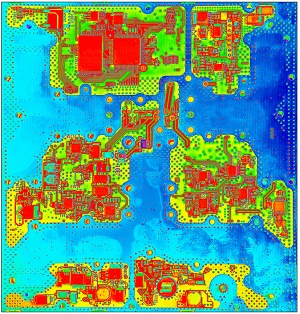
Ventec International is adding to its extensive thermally conductive laminate and pre-preg range with the launch of the VT-5A2, a next-generation best-in-class, high Tg thin-core and pre-preg material.
VT-5A2 is designed for the world's most thermally demanding printed circuit board (PCB) applications such as power converters, hybrid multilayers and high-power electronics with heavy copper designs, providing enhanced signal stability in harsh environments. With VT-5A2, Ventec has created its highest-performance thermally conductive laminate material so far, with a polymer matrix that is fully compatible with Ventec laminates, epoxy or polyimide-based materials including tec-speed®, thus allowing total compatibility in the manufacture of hybrid multilayer boards.
With a thermal conductivity eight times that of FR-4, VT-5A2 delivers class-leading thermal performance and high flowability for perfect encapsulation, allowing for better board design for applications requiring critical thermal management in harsh environments. Customers can choose between thin core and pre-preg variants. VT-5A2 features a thermal conductivity of 2.2 W/m.K, a high Tg of 190°C, best-in-class thermal performance (T260 >60 Minutes, T288 >30 Minutes and T300 >15 Minutes) and M.O.T. up to 150°C. VT-5A2 is lead-free assembly compatible, fulfills RoHS and WEEE requirements and complies with UL94 V0.
The VT-5A2 thermally conductive laminate is manufactured by Ventec using strict quality controlled processes that are certified to AS9100 Revision C, ISO/TS16949 and ISO 9001:2015, and, like all Ventec products, is backed by a fully controlled and managed global supply chain, sales and support network.
About Ventec International
With volume manufacturing facilities and HQ in Suzhou China, Ventec International specializes in advanced copper clad glass reinforced and metal backed substrates for the PCB industry. With distribution locations and manufacturing sites in both the US and Europe, Ventec International is a premier supplier to the global PCB industry. For further information and to request a technical data sheet, please contact sales@ventec-europe.com. Information about Ventec’s solutions and the company’s wide variety of products, is available at www.venteclaminates.com and/or by downloading the Ventec app.
Share on:


Testimonial
"In a year when every marketing dollar mattered, I chose to keep I-Connect007 in our 2025 plan. Their commitment to high-quality, insightful content aligns with Koh Young’s values and helps readers navigate a changing industry. "
Brent Fischthal - Koh YoungSuggested Items
Closing the Loop on PCB Etching Waste
09/09/2025 | Shawn Stone, IECAs the PCB industry continues its push toward greener, more cost-efficient operations, Sigma Engineering’s Mecer System offers a comprehensive solution to two of the industry’s most persistent pain points: etchant consumption and rinse water waste. Designed as a modular, fully automated platform, the Mecer System regenerates spent copper etchants—both alkaline and acidic—and simultaneously recycles rinse water, transforming a traditionally linear chemical process into a closed-loop system.
Driving Innovation: Depth Routing Processes—Achieving Unparalleled Precision in Complex PCBs
09/08/2025 | Kurt Palmer -- Column: Driving InnovationIn PCB manufacturing, the demand for increasingly complex and miniaturized designs continually pushes the boundaries of traditional fabrication methods, including depth routing. Success in these applications demands not only on robust machinery but also sophisticated control functions. PCB manufacturers rely on advanced machine features and process methodologies to meet their precise depth routing goals. Here, I’ll explore some crucial functions that empower manufacturers to master complex depth routing challenges.
Trouble in Your Tank: Minimizing Small-via Defects for High-reliability PCBs
08/27/2025 | Michael Carano -- Column: Trouble in Your TankTo quote the comedian Stephen Wright, “If at first you don’t succeed, then skydiving is not for you.” That can be the battle cry when you find that only small-diameter vias are exhibiting voids. Why are small holes more prone to voids than larger vias when processed through electroless copper? There are several reasons.
The Government Circuit: Navigating New Trade Headwinds and New Partnerships
08/25/2025 | Chris Mitchell -- Column: The Government CircuitAs global trade winds continue to howl, the electronics manufacturing industry finds itself at a critical juncture. After months of warnings, the U.S. Government has implemented a broad array of tariff increases, with fresh duties hitting copper-based products, semiconductors, and imports from many nations. On the positive side, tentative trade agreements with Europe, China, Japan, and other nations are providing at least some clarity and counterbalance.
How Good Design Enables Sustainable PCBs
08/21/2025 | Gerry Partida, Summit InterconnectSustainability has become a key focus for PCB companies seeking to reduce waste, conserve energy, and optimize resources. While many discussions on sustainability center around materials or energy-efficient processes, PCB design is an often overlooked factor that lies at the heart of manufacturing. Good design practices, especially those based on established IPC standards, play a central role in enabling sustainable PCB production. By ensuring designs are manufacturable and reliable, engineers can significantly reduce the environmental impact of their products.