


 The Marketing Minute: Cracking the Code of Technical Marketing
 Trouble in Your Tank: Implementing Direct Metallization in Advanced Substrate Packaging


Hamburg Scientists Develop Novel Nanomaterial with Controllable Optical Properties
March 13, 2017 | Helmholtz-Zentrum GeesthachtEstimated reading time: 3 minutes
Scientists at the Technical University Hamburg (TUHH) and the Helmholtz-Zentrum Geesthacht (HZG) have produced a new optical nanomaterial based on nanoporous gold, which facilitates changes of up to thirty percent in the optical transmission by applying an electrical voltage. The change is incredibly large if one considers that the thickness of the nanomaterial layer is only two hundred nanometres – which is only about five-hundredth the diameter of a human strand of hair.
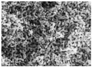
Electron micrographs of the nanoporous gold network.You can see the nanoscale gold wires with the cavities. [Photo: TUHH]
Although it consists of metal, the new nanomaterial does not reflect optical radiation like a normal metal mirror. The nanoscale pore structure results in what is known as a plasmonic-optical metamaterial, which behaves like an absorbing non-metallic material in the visible part of the spectrum and only demonstrates its typical metallic character and the associated reflection properties in near infrared — that is, at longer wavelengths.
The wavelength range at which the nanomaterial absorbs and reflects can be set by manipulating the density of the pore.
Here, in a concrete case, 85% of the total volume consists of pores that are traversed by gold wires measuring only ten nanometres thick. A sponge-like material with a very large inner surface develops. A cube made of this nanoporous gold with an edge length of only four centimetres would have an inner surface measuring the size of a football field. The Hamburg scientists have now filled the material with a water-based electrolyte, which connects an externally applied electrical voltage with the thin gold ligament.
Normally, electron density as well as the optical properties of metals can barely be altered by applying a voltage.
The nanomaterial’s enormous inner surface, however, enables electron density variations in the interconnected metallic wires of up to eight percent by raising and lowering the voltage by only about one volt. This allows the optical transmission to be altered reversibly and on broad bands by up to thirty percent — an adjustable, semi-transparent mirror is created.
The newly developed nanomaterial possesses great potential for splitting water into oxygen and hydrogen by absorbing sunlight. The hydrogen generated without a manmade energy supply is an emission-free regenerative fuel, the first choice in regard to the necessary energy conversion in industrialised societies.
The Hamburg scientists want to make a substantial contribution to creating the necessary scientific technical foundation for supplying environmentally friendly energy at a time when fossil fuels are becoming scarcer, when we are facing the unresolved issue of climate change and in the midst of the current discussion on harmful particulate matter and nitric oxide emissions caused by heating and combustion engines from road traffic.
The research has been carried out within the framework of a successful cooperation for many years by the Technical University Hamburg (TUHH) and the Helmholtz-Zentrum Geesthacht (HZG). This fruitful cooperation is particularly evident in the Research Centre 986 “Tailor-Made Multi-Scale Materials Systems – M³”, jointly run by the TUHH and the HZG since 2012 and funded by the German Research Foundation (DFG) as well as the Centre for High Performance Materials (ZHM), which bundles materials science competence in the greater Hamburg area and was founded for this purpose in 2015, by TUHH and the HZG as well as by participating state governments of Hamburg and Schleswig-Holstein.
“Only the development of complementary skills at the TUHH and the HZG in the fields of photonics and nanoporous metal and the excellent cooperation between the participating scientists enabled us to cope with the range of tasks ahead – from the theoretical description to the electromagnetic simulation to the production of the nanoporous metals and their optical characterisation,” says Prof Manfred Eich. Eich is co-spokesperson of the SFB 986, director of the Institute of Optical and Electronic Materials at the TUHH and head of a working group at the HZG, which is involved in nanophotonic structures for photoelectrochemical hydrogen generation.
Share on:


Testimonial
"In a year when every marketing dollar mattered, I chose to keep I-Connect007 in our 2025 plan. Their commitment to high-quality, insightful content aligns with Koh Young’s values and helps readers navigate a changing industry. "
Brent Fischthal - Koh YoungSuggested Items
Curing and Verification in PCB Shadow Areas
09/17/2025 | Doug Katze, DymaxDesign engineers know a simple truth that often complicates electronics manufacturing: Light doesn’t go around corners. In densely populated PCBs, adhesives and coatings often fail to fully cure in shadowed regions created by tall ICs, connectors, relays, and tight housings.
Marcy’s Musings: Advancing the Advanced Materials Discussion
09/17/2025 | Marcy LaRont -- Column: Marcy's MusingsAs the industry’s most trusted global source of original content about the electronics supply chain, we continually ask you about your concerns, what you care about, and what you most want to learn about. Your responses are insightful and valuable. Thank you for caring enough to provide useful feedback and engage in dialogue.
September 2025 PCB007 Magazine: The Future of Advanced Materials
09/16/2025 | I-Connect007 Editorial TeamMoore’s Law is no more, and the advanced material solutions being developed to grapple with this reality are surprising, stunning, and perhaps a bit daunting. Buckle up for a dive into advanced materials and a glimpse into the next chapters of electronics manufacturing.
I-Connect007 Launches Advanced Electronics Packaging Digest
09/15/2025 | I-Connect007I-Connect007 is pleased to announce the launch of Advanced Electronics Packaging Digest (AEPD), a new monthly digital newsletter dedicated to one of the most critical and rapidly evolving areas of electronics manufacturing: advanced packaging at the interconnect level.
Panasonic Industry will Double the Production Capacity of MEGTRON Multi-layer Circuit Board Materials Over the Next Five Years
09/15/2025 | Panasonic Industry Co., Ltd.Panasonic Industry Co., Ltd., a Panasonic Group company, announced plans for a major expansion of its global production capacity for MEGTRON multi-layer circuit board materials today. The company plans to double its production over the next five years to meet growing demand in the AI server and ICT infrastructure markets.