


 The Marketing Minute: Cracking the Code of Technical Marketing
 Trouble in Your Tank: Implementing Direct Metallization in Advanced Substrate Packaging


Mapping the Effects of Crystal Defects
March 15, 2017 | MITEstimated reading time: 3 minutes
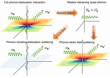
New research offers insights into how crystal dislocations — a common type of defect in materials — can affect electrical and heat transport through crystals, at a microscopic, quantum mechanical level.
Dislocations in crystals are places where the orderly three-dimensional structure of a crystal lattice — whose arrangement of atoms repeats with exactly the same spacing — is disrupted. The effect is as if a knife had sliced through the crystal and then the pieces were stuck back together, askew from their original positions. These defects have a strong effect on phonons, the modes of lattice vibration that play a role in the thermal and electrical properties of the crystals through which they travel. But a precise understanding of the mechanism of the dislocation-phonon interaction has been elusive and controversial, which has slowed progress toward using dislocations to tailor the thermal properties of materials.
A team at MIT has been able to learn important details about how those interactions work, which could inform future efforts to develop thermoelectric devices and other electronic systems. The findings are reported in the journal Nano Letters, in a paper co-authored by postdoc Mingda Li, Department of Mechanical Engineering head Professor Gang Chen, the late Institute Professor Emerita Mildred Dresselhaus, and five others.
Dislocations — which Li describes as “atomic irregularities in a regular crystal” — are very common defects in crystals, and they affect, for example, how heat dissipates through a silicon microchip or how well current flows through a silicon solar panel.
There have been two competing approaches to explaining phonon-dislocation interactions, Li explains, and a few other questions about them have remained unsolved. Now, the MIT team has found a new mathematical approach to analyzing such systems, using a new quasiparticle they formulated called a “dislon,” which is a quantized version of a dislocation, which seems to resolve these longstanding mysteries.
“People have tried to learn how the dislocations change the material properties — the electrical and thermal properties,” Li says. “Before now, there were many empirical models, which need fitting parameters to be complete. There was a long debate about the nature of phonon scattering in dislocations.”
The new theory, Li says, has a different starting point, as it is based on rigorous quantum field theory. It seems to resolve a number of issues, including a debate between two views known as the dynamic and static scattering approaches, showing they are simply
two extreme cases within this new framework. And while both of these approaches fail to explain behavior at the nanoscale, the new approach works well at such scales.
The findings could affect the search for better thermoelectric materials, which can convert heat to electricity. These are used for generating power from waste heat, or providing heaters for car seats. Thermoelectric systems can also provide cooling, for cold-drink chests, for example.
Chen, who is the Carl Richard Soderberg Professor of Power Engineering, attributes the new findings to Li’s initiative. “I didn’t put that much hope in it,” Chen said. “It’s a pretty complex problem: how dislocations affect these very important properties. ... I was very surprised when he came back with this new theory. He started from basic principles and derived a quantum description for it.”
Li and his team have made “a breakthrough by being able to account for the long-range nature of the dislocation strain field, by treating it as a new quantum mechanical object called the dislon,” says Jeffery Snyder, a professor at Northwestern University, who was not connected to this work. “Combining this with the quantum mechanical treatment of the dislon-electron interaction could lead to new strategies to optimize materials by using metallurgical approaches to engineer the structure, type, and location of dislocations within a material.”
“Dislocations have profound effects on properties of materials, but until now the long-range nature of the strain field has prevented direct calculations of dislocation effects,” says David J. Singh, a professor at the University of Missouri who also was not involved in this work. “The quantization developed in this paper goes a long way to solving these problems. I expect that this new formalism will lead to greatly improved understanding of the effects of dislocations on the electrical and thermal properties of materials. This work is a major step forward.”
The research team also included Zhiwei Ding, Jiawei Zhou, and Professor Hong Liu at MIT, and Qingping Meng and Yimei Zhu at Brookhaven National Laboratory. The work was supported by S3TEC, the Energy Frontier Research Center funded by the U.S. Department of Energy’s Office of Basic Energy Sciences, and the Defense Advanced Research Projects Agency of the U.S. Department of Defense.
Share on:


Testimonial
"The I-Connect007 team is outstanding—kind, responsive, and a true marketing partner. Their design team created fresh, eye-catching ads, and their editorial support polished our content to let our brand shine. Thank you all! "
Sweeney Ng - CEE PCBSuggested Items
Curing and Verification in PCB Shadow Areas
09/17/2025 | Doug Katze, DymaxDesign engineers know a simple truth that often complicates electronics manufacturing: Light doesn’t go around corners. In densely populated PCBs, adhesives and coatings often fail to fully cure in shadowed regions created by tall ICs, connectors, relays, and tight housings.
Marcy’s Musings: Advancing the Advanced Materials Discussion
09/17/2025 | Marcy LaRont -- Column: Marcy's MusingsAs the industry’s most trusted global source of original content about the electronics supply chain, we continually ask you about your concerns, what you care about, and what you most want to learn about. Your responses are insightful and valuable. Thank you for caring enough to provide useful feedback and engage in dialogue.
September 2025 PCB007 Magazine: The Future of Advanced Materials
09/16/2025 | I-Connect007 Editorial TeamMoore’s Law is no more, and the advanced material solutions being developed to grapple with this reality are surprising, stunning, and perhaps a bit daunting. Buckle up for a dive into advanced materials and a glimpse into the next chapters of electronics manufacturing.
I-Connect007 Launches Advanced Electronics Packaging Digest
09/15/2025 | I-Connect007I-Connect007 is pleased to announce the launch of Advanced Electronics Packaging Digest (AEPD), a new monthly digital newsletter dedicated to one of the most critical and rapidly evolving areas of electronics manufacturing: advanced packaging at the interconnect level.
Panasonic Industry will Double the Production Capacity of MEGTRON Multi-layer Circuit Board Materials Over the Next Five Years
09/15/2025 | Panasonic Industry Co., Ltd.Panasonic Industry Co., Ltd., a Panasonic Group company, announced plans for a major expansion of its global production capacity for MEGTRON multi-layer circuit board materials today. The company plans to double its production over the next five years to meet growing demand in the AI server and ICT infrastructure markets.