


 The Marketing Minute: Cracking the Code of Technical Marketing
 Trouble in Your Tank: Implementing Direct Metallization in Advanced Substrate Packaging


Better Nanoimages 'Spin' The Path to Improved Magnetic Memory
March 17, 2017 | NISTEstimated reading time: 4 minutes
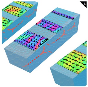
In work that could help make possible a faster, longer-lasting and lower-energy method of data storage for consumers and businesses, researchers at the National Institute of Standards and Technology (NIST) and their colleagues have developed a technique for imaging and studying a promising class of magnetic devices with 10 times more detail than optical microscopes.
Magnetic materials have attracted a growing number of researchers in the quest to more rapidly store and read bits of digital information. In a magnetic system, data is encoded by the direction of the magnetization: A bar magnet with its north pole pointing up can represent the binary code “0,” while the same magnet with its north pole pointing down can represent a “1.” Unlike the standard semiconductor computer chip, magnetic memory devices can retain information even if the power is turned off.
By controlling when and how quickly the magnetization can be flipped without expending significant electrical power, scientists hope to improve an existing technology called Magnetic Random Access Memory, or MRAM, into a leading tool for reading, writing and storing information. MRAM is not yet competitive with other existing methods of data storage such as flash RAM, but offers advantages over present-day technologies such as reduced energy consumption.
To realize the promise of MRAM, researchers are probing the nanometer-scale magnetic structure of thin metal films that have the potential to serve as memory devices in MRAM. At NIST, Ian Gilbert and his colleagues have used a high-resolution electron-imaging technique, developed by physicist John Unguris, to examine the nanostructure of magnetic films before and after their magnetization is reversed.
The technique, scanning electron microscopy with polarization analysis (SEMPA), uses a beam of electrons scattered from a thin film to reveal the nanoscale topography, replete with miniature hills and valleys, of the film’s surface. Electrons ejected from the surface by the incoming electron beam are also detected and separated according to the direction of their spin—a quantum property that endows the charged particles with an intrinsic angular momentum and tiny magnetic field. The direction of the ejected electrons’ spins reveals variations in the sample’s magnetic structure—changes in the direction of magnetization—on a scale about 10 times smaller than seen with an optical microscope.
SEMPA’s ability to discern tiny magnetic structures is critical as engineers fabricate smaller and smaller magnetic memory devices, noted Gilbert. With SEMPA, “we can see these really fine textures in the magnetization,” he said.
Gilbert and his collaborators, which include scientists from NIST and the University of Maryland, also used electron spin to flip the magnetization in their thin-film sample, an alloy of cobalt, iron and boron. By passing a small electric current through an underlying strip of a nonmagnetic metal film such as platinum, the team created a stream of electrons whose spins all point in the same direction. When this stream of electrons, known as a spin current, passed through the magnetic thin film, their spin exerted a small twisting force, or torque, on the magnetic regions of the film. The torque was large enough to rotate and flip the magnetization.
The SEMPA images taken before a current was applied revealed that the direction of the magnetization varied, on the nanoscale, across the thin-film sample. Each small region of the sample has its own preferred axis along which the magnetization points, said Gilbert. The team recently reported its findings in the journal Physical Review B (link is external).
Such nanoscale variations of the magnetization could become crucial to document, said Gilbert, for engineers trying to optimize the performance of a magnetic memory device. The variation in magnetization direction could also affect the ability of electron spin to flip the magnetization.
“Instead of flipping magnetization up or down, the spin current flips the magnetization along whatever its preferred local [spin] axis happens to be,” notes Gilbert. The variation in magnetization direction suggests that materials used for magnetic memory devices may need to be gently heated, a process that aligns nanoscale magnetic domains.
In separate work, NIST scientists Mark Stiles and Vivek Amin, who has a joint appointment with the University of Maryland, focus on the theor describing the torque measured in the SEMPA experiments. There, a stream of polarized electrons generated in a nonmagnetic metal strip interacts with the magnetization of an overlying material. In particular, the team has developed a model that may help determine which group of polarized electrons play the more important role in reversing the direction of magnetization in adjacent material—those originating at the surface of the nonmagnetic material or those from the interior.
The answer could guide the fabrication of more efficient magnetic memory devices. For instance, determining which group of electrons are the dominant actors could suggest ways to minimize the current needed to flip the magnetization, Stiles said.
“Right now, we’re in the process of publicizing the model to experimentalists, trying to get them to use it to better understand their data,” he noted.
Share on:


Testimonial
"The I-Connect007 team is outstanding—kind, responsive, and a true marketing partner. Their design team created fresh, eye-catching ads, and their editorial support polished our content to let our brand shine. Thank you all! "
Sweeney Ng - CEE PCBSuggested Items
MEMS & Imaging Sensors Summit to Spotlight Sensing Revolution for Europe’s Leadership
09/11/2025 | SEMIIndustry experts will gather November 19-20 at the SEMI MEMS & Imaging Sensors Summit 2025 to explore the latest breakthroughs in AI-driven MEMS and imaging optimization, AR/VR technologies, and advanced sensor solutions for critical defence applications.
Direct Imaging System Market Size to Hit $4.30B by 2032, Driven by Increasing Demand for High-Precision PCB Manufacturing
09/11/2025 | Globe NewswireAccording to the SNS Insider, “The Direct Imaging System Market size was valued at $2.21 Billion in 2024 and is projected to reach $4.30 Billion by 2032, growing at a CAGR of 8.68% during 2025-2032.”
I-Connect007’s Editor’s Choice: Five Must-Reads for the Week
07/04/2025 | Marcy LaRont, I-Connect007For our industry, we have seen several bullish market announcements over the past few weeks, including one this week by IDC on the massive growth in the global server market. We’re also closely watching global trade and nearshoring. One good example of successful nearshoring is Rehm Thermal Systems, which celebrates its 10th anniversary in Mexico and the official opening of its new building in Guadalajara.
Driving Innovation: Direct Imaging vs. Conventional Exposure
07/01/2025 | Simon Khesin -- Column: Driving InnovationMy first camera used Kodak film. I even experimented with developing photos in the bathroom, though I usually dropped the film off at a Kodak center and received the prints two weeks later, only to discover that some images were out of focus or poorly framed. Today, every smartphone contains a high-quality camera capable of producing stunning images instantly.
United Electronics Corporation Advances Manufacturing Capabilities with Schmoll MDI-ST Imaging Equipment
06/24/2025 | United Electronics CorporationUnited Electronics Corporation has successfully installed the advanced Schmoll MDI-ST (XL) imaging equipment at their advanced printed circuit board facility. This significant technology investment represents a continued commitment to delivering superior products and maintaining their position as an industry leader in precision PCB manufacturing.