


 The Marketing Minute: Cracking the Code of Technical Marketing
 Trouble in Your Tank: Implementing Direct Metallization in Advanced Substrate Packaging


3-D X-ray Imaging Makes the Finest Details of a Computer Chip Visible
March 17, 2017 | Paul Scherrer InstitutEstimated reading time: 3 minutes
Researchers of the Paul Scherrer Institute PSI have made detailed 3-D images of a commercially available computer chip. This marks the first time a non-destructive method has visualized the paths of a chip’s internal wiring (just 45 nanometres — 45 millionths of a millimetre — wide) and its 34-nanometre-high transistors clearly without distortions or deformations. It is a major challenge for manufacturers to determine if, in the end, the structure of their chips conforms to the specifications. Thus these results represent one important application of an X-ray tomography method that the PSI researchers have been developing for several years. In their experiment, the researchers examined a small piece that they had cut out of the chip beforehand. This sample remained undamaged throughout the measurement. The goal now is to extend the method in such a way that it can be used to examine complete chips. The researchers conducted the experiments at the Swiss Light Source SLS of the Paul Scherrer Institute. They report their results in the latest edition of the journal Nature.
The electrical wiring in many of the electronic chips in our computers and mobile phones are just 45 nanometres wide, the transistors 34 nanometres high. While it is standard practice today to produce structures this delicate, it remains a challenge to measure the exact structure of a finished chip in detail in order to check, for example, if it is built according to the specifications. Nowadays, for such examinations, manufacturers mainly use a method in which layer after layer of the chip is removed and then, after each step, the surface is examined with an electron microscope; this is known as FIB/SEM — focused ion beam/scanning electron microscope imaging.
Now researchers of the Paul Scherrer Institute PSI have used X-rays to achieve non-destructive 3-D imaging of a chip, so that the paths of the conducting lines and the positions of the individual transistors and other circuit elements became clearly visible. The image resolution we were able to produce is comparable to the conventional FIB/SEM examination method, explains Mirko Holler, leader of the project. But we were able to avoid two significant disadvantages: Firstly, the sample remained undamaged, and we have complete information about the three-dimensional structure. Secondly, we avoided distortions of the images that arise in FIB/SEM if the surface of the individual slice is not exactly planar.
Positioned with nanometre precision
For their study, the researchers used a special tomographic method (ptychotomography) that they have developed and enhanced over the course of recent years, and which today offers the worldwide best resolution of 15 nanometres (15 millionths of a millimetre) for examination of a comparably large volume. In the experiment the object to be studied is X-rayed at precisely determined places with light from the Swiss Light Source SLS of the Paul Scherrer Institute — for each illuminated spot a detector then measures the X-ray light pattern after its passage through the sample. The sample is then rotated in small steps and then X-rayed again step-wise after each turn. From the whole set of data obtained, the three-dimensional structure of the sample can be determined. With these measurements, the position of the sample must be known to a precision of just a few nanometres — that was one of the particular challenges in setting up our experimental station, Holler says.
In their experiment the researchers examined small pieces of two chips — a detector chip developed at PSI and a commercially available computer chip. Each piece was about 10 micrometres (that is, 10 thousandths of a millimetre) in size. While the examination of an entire chip with the present measurement setup is not possible, the method’s advantages are brought to bear even in this form, so that the first prospective users have already expressed an interest in conducting measurements at PSI.
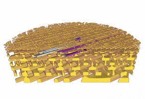
3-D representation of the internal structure of a microchip (an Intel processor). Shown in yellow are the chip’s copper interconnects, which link the individual transistors with each other. The smallest lines shown individually are around 45 nanometres wide (45 millionths of a millimetre); in all, a piece of the processor of around 10 micrometres in diameter (10 thousandths of a millimetre) was examined. The animation is based on X-ray measurements conducted at the Swiss Light Source SLS of the Paul Scherrer Institute. (Video: Paul Scherrer Institute/Mirko Holler)
The goal: to examine entire microchips
“We are currently starting to extend the method in such a way that it can be used to examine entire microchips within an acceptable measurement time. Then it will also be possible to study the same area of a chip multiple times, for example to observe how it changes under external influences”, explains Gabriel Aeppli, head of the Synchrotron Radiation and Nanotechnology Division at the PSI.
Share on:


Testimonial
"In a year when every marketing dollar mattered, I chose to keep I-Connect007 in our 2025 plan. Their commitment to high-quality, insightful content aligns with Koh Young’s values and helps readers navigate a changing industry. "
Brent Fischthal - Koh YoungSuggested Items
Trouble in Your Tank: Implementing Direct Metallization in Advanced Substrate Packaging
09/15/2025 | Michael Carano -- Column: Trouble in Your TankDirect metallization systems based on conductive graphite are gaining popularity throughout the world. The environmental and productivity gains achievable with this process are outstanding. Direct metallization reduces the costs of compliance, waste treatment, and legal issues related to chemical exposure. A graphite-based direct plate system has been devised to address these needs.
Closing the Loop on PCB Etching Waste
09/09/2025 | Shawn Stone, IECAs the PCB industry continues its push toward greener, more cost-efficient operations, Sigma Engineering’s Mecer System offers a comprehensive solution to two of the industry’s most persistent pain points: etchant consumption and rinse water waste. Designed as a modular, fully automated platform, the Mecer System regenerates spent copper etchants—both alkaline and acidic—and simultaneously recycles rinse water, transforming a traditionally linear chemical process into a closed-loop system.
Driving Innovation: Depth Routing Processes—Achieving Unparalleled Precision in Complex PCBs
09/08/2025 | Kurt Palmer -- Column: Driving InnovationIn PCB manufacturing, the demand for increasingly complex and miniaturized designs continually pushes the boundaries of traditional fabrication methods, including depth routing. Success in these applications demands not only on robust machinery but also sophisticated control functions. PCB manufacturers rely on advanced machine features and process methodologies to meet their precise depth routing goals. Here, I’ll explore some crucial functions that empower manufacturers to master complex depth routing challenges.
Trouble in Your Tank: Minimizing Small-via Defects for High-reliability PCBs
08/27/2025 | Michael Carano -- Column: Trouble in Your TankTo quote the comedian Stephen Wright, “If at first you don’t succeed, then skydiving is not for you.” That can be the battle cry when you find that only small-diameter vias are exhibiting voids. Why are small holes more prone to voids than larger vias when processed through electroless copper? There are several reasons.
The Government Circuit: Navigating New Trade Headwinds and New Partnerships
08/25/2025 | Chris Mitchell -- Column: The Government CircuitAs global trade winds continue to howl, the electronics manufacturing industry finds itself at a critical juncture. After months of warnings, the U.S. Government has implemented a broad array of tariff increases, with fresh duties hitting copper-based products, semiconductors, and imports from many nations. On the positive side, tentative trade agreements with Europe, China, Japan, and other nations are providing at least some clarity and counterbalance.