


 Dan's Biz Bookshelf: 'Getting Naked: A Business Fable'
 The Chemical Connection: Common Misconceptions in Wet Processing
 It’s Only Common Sense: Selling to Engineers


Tarnish-Proof Films for Flexible Displays, Touch Screens, Metamaterials
March 22, 2017 | University of MichiganEstimated reading time: 4 minutes
The thinnest, smoothest layer of silver that can survive air exposure has been laid down at the University of Michigan, and it could change the way touchscreens and flat or flexible displays are made.
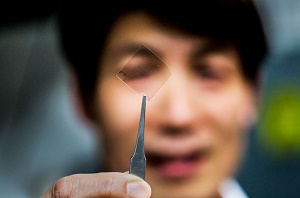
University of Michigan researchers have created a transparent silver film that could be used in touchscreens, flexible displays and other advanced applications. L. Jay Guo, professor of electrical engineering and computer science, holds up a piece of the material. Image credit: Joseph Xu/Michigan Engineering.
It could also help improve computing power, affecting both the transfer of information within a silicon chip and the patterning of the chip itself through metamaterial superlenses.
By combining the silver with a little bit of aluminum, the U-M researchers found that it was possible to produce exceptionally thin, smooth layers of silver that are resistant to tarnishing. They applied an anti-reflective coating to make one thin metal layer up to 92.4 percent transparent.
The team showed that the silver coating could guide light about 10 times as far as other metal waveguides—a property that could make it useful for faster computing. And they layered the silver films into a metamaterial hyperlens that could be used to create dense patterns with feature sizes a fraction of what is possible with ordinary ultraviolet methods, on silicon chips, for instance.
Screens of all stripes need transparent electrodes to control which pixels are lit up, but touchscreens are particularly dependent on them. A modern touch screen is made of a transparent conductive layer covered with a nonconductive layer. It senses electrical changes where a conductive object—such as a finger—is pressed against the screen.
"The transparent conductor market has been dominated to this day by one single material," said L. Jay Guo, professor of electrical engineering and computer science.
This material, indium tin oxide, is projected to become expensive as demand for touch screens continues to grow; there are relatively few known sources of indium, Guo said.
"Before, it was very cheap. Now, the price is rising sharply," he said.
The ultrathin film could make silver a worthy successor.
L. Jay Guo, professor of electrical engineering and computer science at the University of Michigan, and Chengang Ji, a doctoral student in the same department, discuss results from a test of a "stainless" silver film that their research group has created. Image credit: Joseph Xu/Michigan Engineering
Usually, it's impossible to make a continuous layer of silver less than 15 nanometers thick, or roughly 100 silver atoms. Silver has a tendency to cluster together in small islands rather than extend into an even coating, Guo said.
By adding about 6 percent aluminum, the researchers coaxed the metal into a film of less than half that thickness—seven nanometers. What's more, when they exposed it to air, it didn't immediately tarnish as pure silver films do. After several months, the film maintained its conductive properties and transparency. And it was firmly stuck on, whereas pure silver comes off glass with Scotch tape.
In addition to their potential to serve as transparent conductors for touch screens, the thin silver films offer two more tricks, both having to do with silver's unparalleled ability to transport visible and infrared light waves along its surface. The light waves shrink and travel as so-called surface plasmon polaritons, showing up as oscillations in the concentration of electrons on the silver's surface.
Those oscillations encode the frequency of the light, preserving it so that it can emerge on the other side. While optical fibers can't scale down to the size of copper wires on today's computer chips, plasmonic waveguides could allow information to travel in optical rather than electronic form for faster data transfer. As a waveguide, the smooth silver film could transport the surface plasmons over a centimeter—enough to get by inside a computer chip.
The plasmonic capability of the silver film can also be harnessed in metamaterials, which handle light in ways that break the usual rules of optics. Because the light travels with a much shorter wavelength as it moves along the metal surface, the film alone acts as a superlens. Or, to make out even smaller features, the thin silver layers can be alternated with a dielectric material, such as glass, to make a hyperlens.
Such lenses can image objects that are smaller than the wavelength of light, which would blur in an optical microscope. It can also enable laser patterning—such as is used to etch transistors into silicon chips today—to achieve smaller features.
The first author is Cheng Zhang, a recent U-M doctoral graduate in electrical engineering and computer science who now works as a postdoctoral researcher at National Institute of Standards and Technology.
A paper on this research, titled "High-performance Doped Silver Films: Overcoming Fundamental Material Limits for Nanophotonic Applications" is published in Advanced Materials. The study was supported by the National Science Foundation and the Beijing Institute of Collaborative Innovation. U-M has applied for a patent and is seeking partners to bring the technology to market.
Share on:


Suggested Items
Elephantech: For a Greener Tomorrow
04/16/2025 | Marcy LaRont, PCB007 MagazineNobuhiko Okamoto is the global sales and marketing manager for Elephantech Inc., a Japanese startup with a vision to make electronics more sustainable. The company is developing a metal inkjet technology that can print directly on the substrate and then give it a copper thickness by plating. In this interview, he discusses this novel technology's environmental advantages, as well as its potential benefits for the PCB manufacturing and semiconductor packaging segments.
Trouble in Your Tank: Organic Addition Agents in Electrolytic Copper Plating
04/15/2025 | Michael Carano -- Column: Trouble in Your TankThere are numerous factors at play in the science of electroplating or, as most often called, electrolytic plating. One critical element is the use of organic addition agents and their role in copper plating. The function and use of these chemical compounds will be explored in more detail.
IDTechEx Highlights Recyclable Materials for PCBs
04/10/2025 | IDTechExConventional printed circuit board (PCB) manufacturing is wasteful, harmful to the environment and energy intensive. This can be mitigated by the implementation of new recyclable materials and technologies, which have the potential to revolutionize electronics manufacturing.
Connect the Dots: Stop Killing Your Yield—The Hidden Cost of Design Oversights
04/03/2025 | Matt Stevenson -- Column: Connect the DotsI’ve been in this industry long enough to recognize red flags in PCB designs. When designers send over PCBs that look great on the computer screen but have hidden flaws, it can lead to manufacturing problems. I have seen this happen too often: manufacturing delays, yield losses, and designers asking, “Why didn’t anyone tell me sooner?” Here’s the thing: Minor design improvements can greatly impact manufacturing yield, and design oversights can lead to expensive bottlenecks. Here’s how to find the hidden flaws in a design and avoid disaster.
Real Time with... IPC APEX EXPO 2025: Tariffs and Supply Chains in U.S. Electronics Manufacturing
04/01/2025 | Real Time with...IPC APEX EXPOChris Mitchell, VP of Global Government Relations for IPC, discusses IPC's concerns about tariffs on copper and their impact on U.S. electronics manufacturing. He emphasizes the complexity of supply chains and the need for policymakers to understand their effects.