


 Global PCB Connections: Rigid-flex and Flexible PCBs—The Backbone of Modern Electronics
 Flexible Thinking: The Key to a Successful Flex Circuit Design Transfer
 Happy’s Tech Talk #29: Bend-to-Install Semi-flex FR-4


Tarnish-Proof Films for Flexible Displays, Touch Screens, Metamaterials
March 22, 2017 | University of MichiganEstimated reading time: 4 minutes
The thinnest, smoothest layer of silver that can survive air exposure has been laid down at the University of Michigan, and it could change the way touchscreens and flat or flexible displays are made.
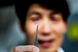
University of Michigan researchers have created a transparent silver film that could be used in touchscreens, flexible displays and other advanced applications. L. Jay Guo, professor of electrical engineering and computer science, holds up a piece of the material. Image credit: Joseph Xu/Michigan Engineering.
It could also help improve computing power, affecting both the transfer of information within a silicon chip and the patterning of the chip itself through metamaterial superlenses.
By combining the silver with a little bit of aluminum, the U-M researchers found that it was possible to produce exceptionally thin, smooth layers of silver that are resistant to tarnishing. They applied an anti-reflective coating to make one thin metal layer up to 92.4 percent transparent.
The team showed that the silver coating could guide light about 10 times as far as other metal waveguides—a property that could make it useful for faster computing. And they layered the silver films into a metamaterial hyperlens that could be used to create dense patterns with feature sizes a fraction of what is possible with ordinary ultraviolet methods, on silicon chips, for instance.
Screens of all stripes need transparent electrodes to control which pixels are lit up, but touchscreens are particularly dependent on them. A modern touch screen is made of a transparent conductive layer covered with a nonconductive layer. It senses electrical changes where a conductive object—such as a finger—is pressed against the screen.
"The transparent conductor market has been dominated to this day by one single material," said L. Jay Guo, professor of electrical engineering and computer science.
This material, indium tin oxide, is projected to become expensive as demand for touch screens continues to grow; there are relatively few known sources of indium, Guo said.
"Before, it was very cheap. Now, the price is rising sharply," he said.
The ultrathin film could make silver a worthy successor.
L. Jay Guo, professor of electrical engineering and computer science at the University of Michigan, and Chengang Ji, a doctoral student in the same department, discuss results from a test of a "stainless" silver film that their research group has created. Image credit: Joseph Xu/Michigan Engineering
Usually, it's impossible to make a continuous layer of silver less than 15 nanometers thick, or roughly 100 silver atoms. Silver has a tendency to cluster together in small islands rather than extend into an even coating, Guo said.
By adding about 6 percent aluminum, the researchers coaxed the metal into a film of less than half that thickness—seven nanometers. What's more, when they exposed it to air, it didn't immediately tarnish as pure silver films do. After several months, the film maintained its conductive properties and transparency. And it was firmly stuck on, whereas pure silver comes off glass with Scotch tape.
In addition to their potential to serve as transparent conductors for touch screens, the thin silver films offer two more tricks, both having to do with silver's unparalleled ability to transport visible and infrared light waves along its surface. The light waves shrink and travel as so-called surface plasmon polaritons, showing up as oscillations in the concentration of electrons on the silver's surface.
Those oscillations encode the frequency of the light, preserving it so that it can emerge on the other side. While optical fibers can't scale down to the size of copper wires on today's computer chips, plasmonic waveguides could allow information to travel in optical rather than electronic form for faster data transfer. As a waveguide, the smooth silver film could transport the surface plasmons over a centimeter—enough to get by inside a computer chip.
The plasmonic capability of the silver film can also be harnessed in metamaterials, which handle light in ways that break the usual rules of optics. Because the light travels with a much shorter wavelength as it moves along the metal surface, the film alone acts as a superlens. Or, to make out even smaller features, the thin silver layers can be alternated with a dielectric material, such as glass, to make a hyperlens.
Such lenses can image objects that are smaller than the wavelength of light, which would blur in an optical microscope. It can also enable laser patterning—such as is used to etch transistors into silicon chips today—to achieve smaller features.
The first author is Cheng Zhang, a recent U-M doctoral graduate in electrical engineering and computer science who now works as a postdoctoral researcher at National Institute of Standards and Technology.
A paper on this research, titled "High-performance Doped Silver Films: Overcoming Fundamental Material Limits for Nanophotonic Applications" is published in Advanced Materials. The study was supported by the National Science Foundation and the Beijing Institute of Collaborative Innovation. U-M has applied for a patent and is seeking partners to bring the technology to market.
Share on:


Testimonial
"Our marketing partnership with I-Connect007 is already delivering. Just a day after our press release went live, we received a direct inquiry about our updated products!"
Rachael Temple - AlltematedSuggested Items
Closing the Loop on PCB Etching Waste
09/09/2025 | Shawn Stone, IECAs the PCB industry continues its push toward greener, more cost-efficient operations, Sigma Engineering’s Mecer System offers a comprehensive solution to two of the industry’s most persistent pain points: etchant consumption and rinse water waste. Designed as a modular, fully automated platform, the Mecer System regenerates spent copper etchants—both alkaline and acidic—and simultaneously recycles rinse water, transforming a traditionally linear chemical process into a closed-loop system.
Driving Innovation: Depth Routing Processes—Achieving Unparalleled Precision in Complex PCBs
09/08/2025 | Kurt Palmer -- Column: Driving InnovationIn PCB manufacturing, the demand for increasingly complex and miniaturized designs continually pushes the boundaries of traditional fabrication methods, including depth routing. Success in these applications demands not only on robust machinery but also sophisticated control functions. PCB manufacturers rely on advanced machine features and process methodologies to meet their precise depth routing goals. Here, I’ll explore some crucial functions that empower manufacturers to master complex depth routing challenges.
Trouble in Your Tank: Minimizing Small-via Defects for High-reliability PCBs
08/27/2025 | Michael Carano -- Column: Trouble in Your TankTo quote the comedian Stephen Wright, “If at first you don’t succeed, then skydiving is not for you.” That can be the battle cry when you find that only small-diameter vias are exhibiting voids. Why are small holes more prone to voids than larger vias when processed through electroless copper? There are several reasons.
The Government Circuit: Navigating New Trade Headwinds and New Partnerships
08/25/2025 | Chris Mitchell -- Column: The Government CircuitAs global trade winds continue to howl, the electronics manufacturing industry finds itself at a critical juncture. After months of warnings, the U.S. Government has implemented a broad array of tariff increases, with fresh duties hitting copper-based products, semiconductors, and imports from many nations. On the positive side, tentative trade agreements with Europe, China, Japan, and other nations are providing at least some clarity and counterbalance.
How Good Design Enables Sustainable PCBs
08/21/2025 | Gerry Partida, Summit InterconnectSustainability has become a key focus for PCB companies seeking to reduce waste, conserve energy, and optimize resources. While many discussions on sustainability center around materials or energy-efficient processes, PCB design is an often overlooked factor that lies at the heart of manufacturing. Good design practices, especially those based on established IPC standards, play a central role in enabling sustainable PCB production. By ensuring designs are manufacturable and reliable, engineers can significantly reduce the environmental impact of their products.