


 Global PCB Connections: Rigid-flex and Flexible PCBs—The Backbone of Modern Electronics
 Flexible Thinking: The Key to a Successful Flex Circuit Design Transfer
 Happy’s Tech Talk #29: Bend-to-Install Semi-flex FR-4


Toward Printable, Sensor-Laden 'Skin' for Robots
March 23, 2017 | MITEstimated reading time: 5 minutes
In this age of smartphones and tablet computers, touch-sensitive surfaces are everywhere. They’re also brittle, as people with cracked phone screens everywhere can attest.
Covering a robot — or an airplane or a bridge — with sensors will require a technology that is both flexible and cost-effective to manufacture in bulk. A team of researchers at MIT’s Computer Science and Artificial Intelligence Laboratory thinks that 3-D printing could be the answer.
In an attempt to demonstrate the feasibility of flexible, printable electronics that combine sensors and processing circuitry and can act on their environments, the researchers have designed and built a device that responds to mechanical stresses by changing the color of a spot on its surface.
The device was inspired by the golden tortoise beetle, or “goldbug,” an insect whose exterior usually appears golden but turns reddish orange if the insect is poked or prodded — that is, mechanically stressed.
“In nature, networks of sensors and interconnects are called sensorimotor pathways,” says Subramanian Sundaram, an MIT graduate student in electrical engineering and computer science (EECS), who led the project. “We were trying to see whether we could replicate sensorimotor pathways inside a 3-D-printed object. So we considered the simplest organism we could find.”
The researchers present their new design in the latest issue of the journal Advanced Materials Technologies. Sundaram is the first author on the paper, and the senior authors are Sundaram’s advisor, Wojciech Matusik, an associate professor of EECS; and Marc Baldo, a professor of EECS and director of the Research Laboratory of Electronics. Joining them on the paper are Pitchaya Sitthi-Amorn, a former postdoc in Matusik’s lab; Ziwen Jiang, an undergraduate EECS student; and David Kim, a technical assistant in Matusik’s Computational Fabrication Group.
Bottom up
Printable electronics, in which flexible circuitry is deposited on some type of plastic substrate, has been a major area of research for decades. But Sundaram says that the ability to print the substrate itself greatly increases the range of devices the technique can yield.
For one thing, the choice of substrate limits the types of materials that can be deposited on top of it. Because a printed substrate could consist of many materials, interlocked in intricate but regular patterns, it broadens the range of functional materials that printable electronics can use.
Printed substrates also open the possibility of devices that, although printed as flat sheets, can fold themselves up into more complex, three-dimensional shapes. Printable robots that spontaneously self-assemble when heated, for instance, are a topic of ongoing research at the CSAIL Distributed Robotics Laboratory, led by Daniela Rus, the Andrew and Erna Viterbi Professor of Electrical Engineering and Computer Science at MIT.
“We believe that only if you’re able to print the underlying substrate can you begin to think about printing a more complex shape,” Sundaram says.
Selective signaling
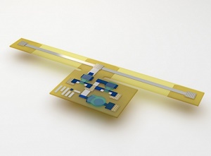
The MIT researchers’ new device is approximately T-shaped, but with a wide, squat base and an elongated crossbar. The crossbar is made from an elastic plastic, with a strip of silver running its length; in the researchers’ experiments, electrodes were connected to the crossbar’s ends. The base of the T is made from a more rigid plastic. It includes two printed transistors and what the researchers call a “pixel,” a circle of semiconducting polymer whose color changes when the crossbars stretch, modifying the electrical resistance of the silver strip.
In fact, the transistors and the pixel are made from the same material; the transistors also change color slightly when the crossbars stretch. The effect is more dramatic in the pixel, however, because the transistors amplify the electrical signal from the crossbar. Demonstrating working transistors was essential, Sundaram says, because large, dense sensor arrays require some capacity for onboard signal processing.
“You wouldn’t want to connect all the sensors to your main computer, because then you would have tons of data coming in,” he says. “You want to be able to make clever connections and to select just the relevant signals.”
To build the device, the researchers used the MultiFab, a custom 3-D printer developed by Matusik’s group. The MultiFab already included two different “print heads,” one for emitting hot materials and one for cool, and an array of ultraviolet light-emitting diodes. Using ultraviolet radiation to “cure” fluids deposited by the print heads produces the device’s substrate.
Sundaram added a copper-and-ceramic heater, which was necessary to deposit the semiconducting plastic: The plastic is suspended in a fluid that’s sprayed onto the device surface, and the heater evaporates the fluid, leaving behind a layer of plastic only 200 nanometers thick.
Fluid boundaries
A transistor consists of semiconductor channel on top of which sits a “gate,” a metal wire that, when charged, generates an electric field that switches the semiconductor between its electrically conductive and nonconductive states. In a standard transistor, there’s an insulator between the gate and the semiconductor, to prevent the gate current from leaking into the semiconductor channel.
The transistors in the MIT researchers’ device instead separate the gate and the semiconductor with a layer of water containing a potassium salt. Charging the gate drives potassium ions into the semiconductor, changing its conductivity.
The layer of saltwater lowers the device’s operational voltage, so that it can be powered with an ordinary 1.5-volt battery. But it does render the device less durable. “I think we can probably get it to work stably for two months, maybe,” Sundaram says. “One option is to replace that liquid with something between a solid and a liquid, like a hydrogel, perhaps. But that’s something we would work on later. This is an initial demonstration.”
“I am very impressed with both the concept and the realization of the system,” says Hagen Klauk, who leads the Organic Electronic Research Group at the Max Planck Institute for Solid State Research, in Stuttgart, Germany. “The approach of printing an entire optoelectronic system — including the substrate and all the components — by depositing all the materials, including solids and liquids, by 3-D printing is certainly novel, interesting, and useful, and the demonstration of the functional system confirms that the approach is also doable. By fabricating the substrate on the fly, the approach is particularly useful for improvised manufacturing environments where dedicated substrate materials may not be available.”
Share on:


Testimonial
"The I-Connect007 team is outstanding—kind, responsive, and a true marketing partner. Their design team created fresh, eye-catching ads, and their editorial support polished our content to let our brand shine. Thank you all! "
Sweeney Ng - CEE PCBSuggested Items
Closing the Loop on PCB Etching Waste
09/09/2025 | Shawn Stone, IECAs the PCB industry continues its push toward greener, more cost-efficient operations, Sigma Engineering’s Mecer System offers a comprehensive solution to two of the industry’s most persistent pain points: etchant consumption and rinse water waste. Designed as a modular, fully automated platform, the Mecer System regenerates spent copper etchants—both alkaline and acidic—and simultaneously recycles rinse water, transforming a traditionally linear chemical process into a closed-loop system.
Driving Innovation: Depth Routing Processes—Achieving Unparalleled Precision in Complex PCBs
09/08/2025 | Kurt Palmer -- Column: Driving InnovationIn PCB manufacturing, the demand for increasingly complex and miniaturized designs continually pushes the boundaries of traditional fabrication methods, including depth routing. Success in these applications demands not only on robust machinery but also sophisticated control functions. PCB manufacturers rely on advanced machine features and process methodologies to meet their precise depth routing goals. Here, I’ll explore some crucial functions that empower manufacturers to master complex depth routing challenges.
Trouble in Your Tank: Minimizing Small-via Defects for High-reliability PCBs
08/27/2025 | Michael Carano -- Column: Trouble in Your TankTo quote the comedian Stephen Wright, “If at first you don’t succeed, then skydiving is not for you.” That can be the battle cry when you find that only small-diameter vias are exhibiting voids. Why are small holes more prone to voids than larger vias when processed through electroless copper? There are several reasons.
The Government Circuit: Navigating New Trade Headwinds and New Partnerships
08/25/2025 | Chris Mitchell -- Column: The Government CircuitAs global trade winds continue to howl, the electronics manufacturing industry finds itself at a critical juncture. After months of warnings, the U.S. Government has implemented a broad array of tariff increases, with fresh duties hitting copper-based products, semiconductors, and imports from many nations. On the positive side, tentative trade agreements with Europe, China, Japan, and other nations are providing at least some clarity and counterbalance.
How Good Design Enables Sustainable PCBs
08/21/2025 | Gerry Partida, Summit InterconnectSustainability has become a key focus for PCB companies seeking to reduce waste, conserve energy, and optimize resources. While many discussions on sustainability center around materials or energy-efficient processes, PCB design is an often overlooked factor that lies at the heart of manufacturing. Good design practices, especially those based on established IPC standards, play a central role in enabling sustainable PCB production. By ensuring designs are manufacturable and reliable, engineers can significantly reduce the environmental impact of their products.
Copyright © I-Connect007 | IPC Publishing Group Inc. All rights reserved.
Log in