


 The Marketing Minute: Cracking the Code of Technical Marketing
 Trouble in Your Tank: Implementing Direct Metallization in Advanced Substrate Packaging


Ultrafast Measurements Explain Quantum Dot Voltage Drop
March 24, 2017 | Los Alamos National LaboratoryEstimated reading time: 3 minutes
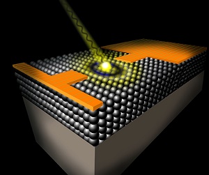
Solar cells and photodetectors could soon be made from new types of materials based on semiconductor quantum dots, thanks to new insights based on ultrafast measurements capturing real-time photoconversion processes.
“Our latest ultrafast electro-optical spectroscopy studies provide unprecedented insights into the photophysics of quantum dots,” said lead researcher Victor Klimov, a physicist specializing in semiconductor nanocrystals at Los Alamos National Laboratory, “and this new information helps perfect the materials’ properties for applications in practical photoconversion devices. Our new experimental technique allows us to follow a chain of events launched by femtosecond laser pulses and pin down processes responsible for efficiency losses during transformation of incident light into electrical current.”
Photoconversion is a process wherein the energy of a photon, or quantum of light, is converted into other forms of energy, for example, chemical or electrical. Semiconductor quantum dots are chemically synthesized crystalline nanoparticles that have been studied for more than three decades in the context of various photoconversion schemes including photovoltaics (generation of photo-electricity) and photo-catalysis (generation of “solar fuels”). The appeal of quantum dots comes from the unmatched tunability of their physical properties, which can be adjusted by controlling the size, shape and composition of the dots.
At Los Alamos, the research connects to the institutional mission of solving national security challenges through scientific excellence, in this case focusing on novel physical principles for highly efficient photoconversion, charge manipulation in exploratory device structures and novel nanomaterials.
The interest in quantum dots as solar-cell materials has been motivated by their tunable optical spectra as well as interesting new physics such as high-efficiency carrier multiplication, that is, generation of multiple electron-hole pairs by single photons. This effect, discovered by Los Alamos researchers in 2004, resulted in the surge of activities in the area of quantum dot solar cells that quickly pushed the efficiencies of practical devices to more than 10 percent.
Further progress in this area has been by hindered by the challenge of understanding the mechanisms of electrical conductance in quantum dot solids and the processes that limit the charge transport distance. One specific and persistent challenge of great importance from the standpoint of photovoltaic (PV) applications, Klimov said, is understanding the reasons underlying a considerable loss in photovoltage compared to predicted theoretical limits—a problem with quantum dot solar cells known as a “photovoltage deficit.” Los Alamos researchers at the Center for Advanced Solar Photophysics (CASP) helps answer some of the above questions.
By applying a combination of ultrafast optical and electrical techniques, the Los Alamos scientists have been able to resolve step-by-step a sequence of events involved in photoconversion in quantum dot films from generation of an exciton to electron-hole separation, dot-to-dot charge migration and finally recombination.
The high temporal resolution of these measurements (better than one billionth of a second) enabled the team to reveal the cause of a large drop of the electron energy, which results from very fast electron trapping by defect-related states. In the case of practical devices, this process would result in reduced photovoltage. The newly conducted studies establish the exact time scale of this problematic trapping process and suggest that a moderate (less than ten-fold) improvement in the electron mobility should allow for collecting photogenerated charge carriers prior to their relaxation into lower-energy states. This would produce a dramatic boost in the photovoltage and therefore increase the overall device efficiency.
Another interesting effect revealed by these studies is the influence of electron and hole “spins” on photoconductance. Usually spin properties of particles (they can be thought of as the rate and direction of particle rotation around its axis) are invoked in the case of interactions with a magnetic field. However, previously it was found that even a weak interaction between spins of an electron and a hole (so-called "spin-exchange" interaction) has a dramatic effect on light emission from the quantum dots.
The present measurements reveal that these interactions also affect the process of electron-hole separation between adjacent dots in quantum-dot solids. Specifically these studies suggest that future efforts on high-sensitivity quantum-dot photodetectors should take into consideration the effect of exchange blockade, which otherwise might inhibit low-temperature photoconductance.
Quantum dot materials have been at the heart of research at the Los Alamos Center for Advanced Solar Photophysics, which has investigated their application to solar-energy technologies such as luminescent sunlight collectors for solar windows and low-cost PV cells processed from quantum dot solutions.
About Los Alamos National Laboratory
Los Alamos National Laboratory, a multidisciplinary research institution engaged in strategic science on behalf of national security, is operated by Los Alamos National Security, LLC, a team composed of Bechtel National, the University of California, BWXT Government Group, and URS, an AECOM company, for the Department of Energy’s National Nuclear Security Administration.
Share on:


Testimonial
"The I-Connect007 team is outstanding—kind, responsive, and a true marketing partner. Their design team created fresh, eye-catching ads, and their editorial support polished our content to let our brand shine. Thank you all! "
Sweeney Ng - CEE PCBSuggested Items
Electra’s ElectraJet EMJ110 Inkjet Soldermask Now in Black & Blue at Sunrise Electronics
09/08/2025 | Electra Polymers LtdFollowing the successful deployment of Electra’s Green EMJ110 Inkjet Soldermask on KLA’s Orbotech Neos™ platform at Sunrise Electronics in Elk Grove Village, Illinois, production has now moved beyond green.
Magnachip Semiconductor Announces YJ Kim to Step Down as CEO; Current Board Chairman Camillo Martino Appointed Interim CEO
08/14/2025 | PR NewswireMagnachip Semiconductor Corporation today announced that YJ Kim has agreed to step down as CEO and as a member of the Board of Directors, effective immediately. Camillo Martino, Chairman of the Board of Directors, has also been appointed Interim Chief Executive Officer, effective immediately.
Bell to Build X-Plane for Phase 2 of DARPA Speed and Runway Independent Technologies (SPRINT) X-Plane Program
07/09/2025 | Bell Textron Inc.Bell Textron Inc., a Textron Inc. company, has been down-selected for Phase 2 of Defense Advanced Research Projects Agency (DARPA) Speed and Runway Independent Technologies (SPRINT) X-Plane program with the objective to complete design, construction, ground testing and certification of an X-plane demonstrator.
Nolan’s Notes: Moving Forward With Confidence
06/03/2025 | Nolan Johnson -- Column: Nolan's NotesWe’re currently enjoying a revitalized and dynamic EMS provider market with significant growth potential. Since December 2024, the book-to-bill has been extremely strong and growing. Starting with a ratio of 1.24 in December, book-to-bill has continued to accelerate to a 1.41 in April. Yet, there is a global economic restructuring taking place. To say that the back-and-forth with tariffs and trade deals makes for an uncertain market is an understatement. While we may be in a 90-day tariff pause among leading economic nations, the deadline is quickly approaching and that leaves many of you feeling unsettled about what to expect.
Mycronic High Flex Changes Division Name to PCB Assembly Solutions
05/20/2025 | MycronicMycronic AB, the leading Sweden-based electronics assembly solutions provider, announced that its division formerly known as High Flex will now operate under the name PCB Assembly Solutions.