


 The Marketing Minute: Cracking the Code of Technical Marketing
 Trouble in Your Tank: Implementing Direct Metallization in Advanced Substrate Packaging


Multi-Parameter Microscopy Aids Design of Improved Optoelectronic Devices
March 24, 2017 | National Physical LaboratoryEstimated reading time: 1 minute
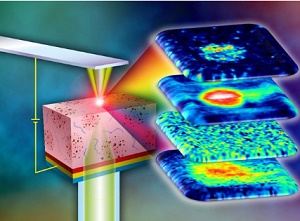
The National Physical Laboratory (NPL) has developed a novel measurement method, providing simultaneous topographical, electrical, chemical and optical microscopy (STEOM) at the nanoscale for the first time. The new method can be used to optimise the performance of optoelectronic devices such as organic solar cells, sensors and transistors.
The STEOM apparatus for multi-parameter characterisation of optoelectronic devices at the nanoscale
As part of an international collaboration, NPL researchers demonstrated the direct application of the new method to the optimisation of organic solar cells. Transparent, flexible and low-cost organic solar cells could offer a solution to large-scale, low-carbon energy generation. However, a lack of analytical techniques that can simultaneously probe device properties at the nanoscale has presented a major obstacle to their optimisation.
The new STEOM method developed at NPL addresses this problem, providing simultaneous measurements of topography and electrical, chemical and optical properties, while also being non-destructive, causing no damage to the samples being measured. The breakthrough was achieved by combining plasmonic optical signal enhancement with electrical-mode scanning probe microscopy. This allows the relationship between surface morphology, chemical composition and current generation in operating organic solar cells to be explored at the nanoscale for the first time.
The team demonstrated that information gained using the method can successfully explain the performance of organic solar cells in terms of the nanoscale composition of their active surface layer, and could be used to identify the best routes for device optimisation. In addition to organic solar cells, the method can be applied to a range of different problems where nanoscale electronic properties are influenced by surface composition and could consequently be used to guide the design of improved optoelectronic devices, from sensors to LEDs.
Share on:


Testimonial
"We’re proud to call I-Connect007 a trusted partner. Their innovative approach and industry insight made our podcast collaboration a success by connecting us with the right audience and delivering real results."
Julia McCaffrey - NCAB GroupSuggested Items
U.S. Uses Secret Trackers to Trace AI Chips Diverted to China, Sources Say
08/18/2025 | I-Connect007 Editorial TeamTwo sources told Reuters that U.S. authorities have secretly placed location trackers in some advanced chip shipments they see as at high risk of illegal diversion to China. They said the trackers are intended to locate AI chips that are sent to locations restricted by U.S. export laws, but authorities only examine some shipments.
Happy’s Tech Talk #38: Novel Metallization for UHDI
05/07/2025 | Happy Holden -- Column: Happy’s Tech TalkI have been involved in high-density electronics substrates since 1970 when I joined Hewlett-Packard’s RF semiconductor group after college. Figure 1 shows the difference between trace/space lithography for substrates and silicon starting in 1970. My projects involved sapphire circuits for RF devices, but the figure displays the state of PCBs and integrated CMOS circuits and their packaging, not discreet RF devices. Even then, semiconductors were 50X higher density.
New Database of Materials Accelerates Electronics Innovation
05/05/2025 | ACN NewswireIn a collaboration between Murata Manufacturing Co., Ltd., and the National Institute for Materials Science (NIMS), researchers have built a comprehensive new database of dielectric material properties curated from thousands of scientific papers.
New Database of Materials Accelerates Electronics Innovation
05/02/2025 | ACN NewswireIn a collaboration between Murata Manufacturing Co., Ltd., and the National Institute for Materials Science (NIMS), researchers have built a comprehensive new database of dielectric material properties curated from thousands of scientific papers.
Micron Announces Business Unit Reorganization to Capitalize on AI Growth Across All Market Segments
04/23/2025 | MicronMicron Technology, Inc., a leader in innovative memory and storage solutions, announced a market segment-based reorganization of its business units to capitalize on the transformative growth driven by AI, from data centers to edge devices.