


 The Marketing Minute: Cracking the Code of Technical Marketing
 Trouble in Your Tank: Implementing Direct Metallization in Advanced Substrate Packaging


Graphene-Based Neural Probes Probe Brain Activity in High Resolution
March 30, 2017 | Graphene FlagshipEstimated reading time: 3 minutes
Measuring brain activity with precision is essential to developing further understanding of diseases such as epilepsy and disorders that affect brain function and motor control. Neural probes with high spatial resolution are needed for both recording and stimulating specific functional areas of the brain. Now, researchers from the Graphene Flagship have developed a new device for recording brain activity in high resolution while maintaining excellent signal to noise ratio (SNR). Based on graphene field-effect transistors, the flexible devices open up new possibilities for the development of functional implants and interfaces.
The Graphene Flagship’s Biomedical Technologies Work Package explores the use of graphene and related materials in biomedical implant devices such as neural implants for recording and stimulating electrical activity, and targeted drug delivery. Graphene’s biocompatibility, chemical stability and flexibility – alongside its excellent electrical properties – make it attractive for use in medical devices. “Mechanical compliance is an important requirement for safe neural probes and interfaces,” said Jose Antonio Garrido, who led the research at ICN2. “Currently, the focus is on ultra-soft materials that can adapt conformally to the brain surface.”
Measuring brain activity
The devices were used to record the large signals generated by pre-epileptic activity in rats, as well as the smaller levels of brain activity during sleep and in response to visual light stimulation. These types of activities lead to much smaller electrical signals, and are at the level of typical brain activity. The graphene transistor probes showed excellent performance, with a high SNR and good spatial discrimination of the brain activity.
Neural activity is detected through the electric fields generated when neurons fire. These fields are highly localised, so having ultra-small measuring devices that can be densely packed is important for accurate brain readings. The graphene-based probes are competitive with state-of-the-art platinum electrode arrays and have the benefits of intrinsic signal amplification and a better signal-to-noise performance when scaled down to very small sizes. This will allow for more densely packed and higher resolution probes, vital for precision mapping of brain activity. The inherent amplification property of the transistor also removes the need for a preamplification close to the probe – a requirement for metal electrodes.
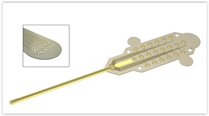
Graphene neural probes
The neural probes are placed directly on the surface of the brain, so safety is of paramount importance for the development of graphene-based neural implant devices. “Graphene is one of the few materials that allows recording in a transistor configuration and simultaneously complies with all other requirements for neural probes such as flexibility, biocompability and chemical stability.” said Benno Blaschke of TU Munich, first author of the research. Importantly, the researchers determined that the graphene-based probes are non-toxic, and did not induce any significant inflammation. Graphene-containing implants should be long-lasting and safe – key characteristics of long-term therapeutic devices.
An array of 16 graphene-based transistors, each with an active area less than the cross section of a human hair, are arranged on a flexible substrate to form the probe. “Although graphene is ideally suited for flexible electronics, it was a great challenge to transfer our fabrication process from rigid substrates to flexible ones,” said Blaschke. “The next step is to optimize the wafer-scale fabrication process and improve device flexibility and stability.”
Future implant technology
This work represents a first step towards the use of graphene in research as well as clinical neural devices, showing that graphene-based technologies can deliver the high resolution and high SNR needed for these applications. “Graphene neural interfaces have shown already a great potential, but we have to improve on the yield and homogeneity of the device production in order to advance towards a real technology,” said Garrido, who is also the Deputy of the Graphene Flagship Biomedical Technologies work package. “Once we have demonstrated the proof of concept in animal studies, the next goal will be to work towards the first human clinical trial with graphene devices during intraoperative mapping of the brain. This means addressing all regulatory issues associated to medical devices such as safety, biocompatibility, etc.”
Devices implanted in the brain as neural prosthesis for therapeutic brain stimulation technologies and interfaces for sensory and motor devices, such as artificial limbs, are an important goal for improving quality of life for patients. Andrea Ferrari, Science and Technology Officer and Chair of the Management Panel of the Graphene Flagship, added "We are pleased to see this promising result from the newly formed work-package on Biomedical Technologies. This was created to exploit the short and long term potential of graphene and related materials in this high growth area, with great potential benefits for society."
Share on:


Testimonial
"Advertising in PCB007 Magazine has been a great way to showcase our bare board testers to the right audience. The I-Connect007 team makes the process smooth and professional. We’re proud to be featured in such a trusted publication."
Klaus Koziol - atgSuggested Items
Curing and Verification in PCB Shadow Areas
09/17/2025 | Doug Katze, DymaxDesign engineers know a simple truth that often complicates electronics manufacturing: Light doesn’t go around corners. In densely populated PCBs, adhesives and coatings often fail to fully cure in shadowed regions created by tall ICs, connectors, relays, and tight housings.
Marcy’s Musings: Advancing the Advanced Materials Discussion
09/17/2025 | Marcy LaRont -- Column: Marcy's MusingsAs the industry’s most trusted global source of original content about the electronics supply chain, we continually ask you about your concerns, what you care about, and what you most want to learn about. Your responses are insightful and valuable. Thank you for caring enough to provide useful feedback and engage in dialogue.
September 2025 PCB007 Magazine: The Future of Advanced Materials
09/16/2025 | I-Connect007 Editorial TeamMoore’s Law is no more, and the advanced material solutions being developed to grapple with this reality are surprising, stunning, and perhaps a bit daunting. Buckle up for a dive into advanced materials and a glimpse into the next chapters of electronics manufacturing.
I-Connect007 Launches Advanced Electronics Packaging Digest
09/15/2025 | I-Connect007I-Connect007 is pleased to announce the launch of Advanced Electronics Packaging Digest (AEPD), a new monthly digital newsletter dedicated to one of the most critical and rapidly evolving areas of electronics manufacturing: advanced packaging at the interconnect level.
Panasonic Industry will Double the Production Capacity of MEGTRON Multi-layer Circuit Board Materials Over the Next Five Years
09/15/2025 | Panasonic Industry Co., Ltd.Panasonic Industry Co., Ltd., a Panasonic Group company, announced plans for a major expansion of its global production capacity for MEGTRON multi-layer circuit board materials today. The company plans to double its production over the next five years to meet growing demand in the AI server and ICT infrastructure markets.