


 The Marketing Minute: Cracking the Code of Technical Marketing
 Trouble in Your Tank: Implementing Direct Metallization in Advanced Substrate Packaging


Beyond Graphene: Advances Make Reduced Graphene Oxide Electronics Feasible
March 30, 2017 | NC State UniversityEstimated reading time: 1 minute
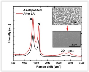
Researchers at North Carolina State University have developed a technique for converting positively charged (p-type) reduced graphene oxide (rGO) into negatively charged (n-type) rGO, creating a layered material that can be used to develop rGO-based transistors for use in electronic devices.
“Graphene is extremely conductive, but is not a semiconductor; graphene oxide has a bandgap like a semiconductor, but does not conduct well at all – so we created rGO,” says Jay Narayan, the John C. Fan Distinguished Chair Professor of Materials Science and Engineering at NC State and corresponding author of a paper describing the work. “But rGO is p-type, and we needed to find a way to make n-type rGO. And now we have it for next-generation, two-dimensional electronic devices.”
Specifically, Narayan and Anagh Bhaumik – a Ph.D. student in his lab – demonstrated two things in this study. First, they were able to integrate rGO onto sapphire and silicon wafers – across the entire wafer.
Second, the researchers used high-powered laser pulses to disrupt chemical groups at regular intervals across the wafer. This disruption moved electrons from one group to another, effectively converting p-type rGO to n-type rGO. The entire process is done at room temperature and pressure using high-power nanosecond laser pulses, and is completed in less than one-fifth of a microsecond. The laser radiation annealing provides a high degree of spatial and depth control for creating the n-type regions needed to create p-n junction-based two-dimensional electronic devices.
The end result is a wafer with a layer of n-type rGO on the surface and a layer of p-type rGO underneath.
This is critical, because the p-n junction, where the two types meet, is what makes the material useful for transistor applications.
Share on:


Testimonial
"Advertising in PCB007 Magazine has been a great way to showcase our bare board testers to the right audience. The I-Connect007 team makes the process smooth and professional. We’re proud to be featured in such a trusted publication."
Klaus Koziol - atgSuggested Items
A.R.T. Invests in Latest Equipment to Further Enhance Electronics Training Facilities
09/17/2025 | A.R.T. Ltd.Advanced Rework Technology Ltd. (A.R.T.), a leading independent IPC-accredited training provider, has announced a series of new equipment investments at its state-of-the-art training centre.
Richardson Electronics Appoints Daniel Albers to Drive Made-in-USA Contract Manufacturing Expansion
09/17/2025 | Globe NewswireRichardson Electronics, Ltd., a global provider of engineered solutions for the green energy, power management, and custom display markets, announced the appointment of Daniel Albers to spearhead business development for its expanded, Made-in-USA contract manufacturing efforts.
STMicroelectronics to Advance Next-generation Chip Manufacturing Technology with New PLP Pilot Line in Tours, France
09/17/2025 | STMicroelectronicsSTMicroelectronics, a global semiconductor leader serving customers across the spectrum of electronics applications, today announced new details regarding the development of the next generations of Panel-Level Packaging (PLP) technology through a pilot line in its Tours site, France, which is expected to be operational in Q3 2026.
Indium President and CEO to Deliver ELCINA CEO Forum Keynote at Productronica India
09/17/2025 | Indium CorporationIndium Corporation President and CEO Ross Berntson will deliver the Electronic Industries Association of India (ELCINA) CEO Forum keynote at Productronica India, to be held September 17-19 in Bengaluru, India.
TTCI and The Training Connection Strengthen Electronics Manufacturing with Test Services and Training at PCB West 2025
09/16/2025 | The Test Connection Inc.The Test Connection Inc. (TTCI), a trusted provider of electronic test and manufacturing solutions, and The Training Connection LLC (TTC-LLC) will exhibit at PCB West 2025, taking place Wednesday, October 1, 2025, at the Santa Clara Convention Center in California. Visitors are invited to Booth 113 to explore the companies’ complementary expertise in test engineering services and workforce development for the electronics industry.