


 The Marketing Minute: Cracking the Code of Technical Marketing
 Trouble in Your Tank: Implementing Direct Metallization in Advanced Substrate Packaging


New Technique Produces Highly Conductive Graphene Wafers
April 4, 2017 | MITEstimated reading time: 4 minutes
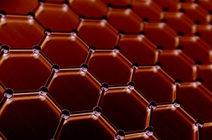
From an electron’s point of view, graphene must be a hair-raising thrill ride. For years, scientists have observed that electrons can blitz through graphene at velocities approaching the speed of light, far faster than they can travel through silicon and other semiconducting materials.
Graphene, therefore, has been touted as a promising successor to silicon, with the potential to enable faster, more efficient electronic and photonic devices.
But manufacturing pristine graphene — a single, perfectly flat, ultrathin sheet of carbon atoms, precisely aligned and linked together like chickenwire — is extremely difficult. Conventional fabrication processes often generate wrinkles, which can derail an electron’s bullet-train journey, significantly limiting graphene’s electrical performance.
Now engineers at MIT have found a way to make graphene with fewer wrinkles, and to iron out the wrinkles that do appear. After fabricating and then flattening out the graphene, the researchers tested its electrical conductivity. They found each wafer exhibited uniform performance, meaning that electrons flowed freely across each wafer, at similar speeds, even across previously wrinkled regions.
In a paper published today in the Proceedings of the National Academy of Sciences, the researchers report that their techniques successfully produce wafer-scale, “single-domain” graphene — single layers of graphene that are uniform in both atomic arrangement and electronic performance.
“For graphene to play as a main semiconductor material for industry, it has to be single-domain, so that if you make millions of devices on it, the performance of the devices is the same in any location,” says Jeehwan Kim, the Class of 1947 Career Development Assistant Professor in the departments of Mechanical Engineering and Materials Science and Engineering at MIT. “Now we can really produce single-domain graphene at wafer scale.”
Kim’s co-authors include Sanghoon Bae, Samuel Cruz, and Yunjo Kim from MIT, along with researchers from IBM, the University of California at Los Angeles, and Kyungpook National University in South Korea.
A patchwork of wrinkles
The most common way to make graphene involves chemical vapor deposition, or CVD, a process in which carbon atoms are deposited onto a crystalline substrate such as copper foil. Once the copper foil is evenly coated with a single layer of carbon atoms, scientists submerge the entire thing in acid to etch away the copper. What remains is a single sheet of graphene, which researchers then pull out from the acid.
The CVD process can produce relatively large, macroscropic wrinkles in graphene, due to the roughness of the underlying copper itself and the process of pulling the graphene out from the acid. The alignment of carbon atoms is not uniform across the graphene, creating a “polycrystalline” state in which graphene resembles an uneven, patchwork terrain, preventing electrons from flowing at uniform rates.
In 2013, while working at IBM, Kim and his colleagues developed a method to fabricate wafers of single-crystalline graphene, in which the orientation of carbon atoms is exactly the same throughout a wafer.
Rather than using CVD, his team produced single-crystalline graphene from a silicon carbide wafer with an atomically smooth surface, albeit with tiny, step-like wrinkles on the order of several nanometers. They then used a thin sheet of nickel to peel off the topmost graphene from the silicon carbide wafer, in a process called layer-resolved graphene transfer.
Ironing charges
In their new paper, Kim and his colleagues discovered that the layer-resolved graphene transfer irons out the steps and tiny wrinkles in silicon carbide-fabricated graphene. Before transferring the layer of graphene onto a silicon wafer, the team oxidized the silicon, creating a layer of silicon dioxide that naturally exhibits electrostatic charges. When the researchers then deposited the graphene, the silicon dioxide effectively pulled graphene’s carbon atoms down onto the wafer, flattening out its steps and wrinkles.
Kim says this ironing method would not work on CVD-fabricated graphene, as the wrinkles generated through CVD are much larger, on the order of several microns.
“The CVD process creates wrinkles that are too high to be ironed out,” Kim notes. “For silicon carbide graphene, the wrinkles are just a few nanometers high, short enough to be flattened out.”
To test whether the flattened, single-crystalline graphene wafers were single-domain, the researchers fabricated tiny transistors on multiple sites on each wafer, including across previously wrinkled regions.
“We measured electron mobility throughout the wafers, and their performance was comparable,” Kim says. “What’s more, this mobility in ironed graphene is two times faster. So now we really have single-domain graphene, and its electrical quality is much higher [than graphene-attached silicon carbide].”
Kim says that while there are still challenges to adapting graphene for use in electronics, the group’s results give researchers a blueprint for how to reliably manufacture pristine, single-domain, wrinkle-free graphene at wafer scale.
“If you want to make any electronic device using graphene, you need to work with single-domain graphene,” Kim says. “There’s still a long way to go to make an operational transistor out of graphene. But we can now show the community guidelines for how you can make single-crystalline, single-domain graphene.”
Share on:


Testimonial
"In a year when every marketing dollar mattered, I chose to keep I-Connect007 in our 2025 plan. Their commitment to high-quality, insightful content aligns with Koh Young’s values and helps readers navigate a changing industry. "
Brent Fischthal - Koh YoungSuggested Items
Trouble in Your Tank: Implementing Direct Metallization in Advanced Substrate Packaging
09/15/2025 | Michael Carano -- Column: Trouble in Your TankDirect metallization systems based on conductive graphite are gaining popularity throughout the world. The environmental and productivity gains achievable with this process are outstanding. Direct metallization reduces the costs of compliance, waste treatment, and legal issues related to chemical exposure. A graphite-based direct plate system has been devised to address these needs.
Closing the Loop on PCB Etching Waste
09/09/2025 | Shawn Stone, IECAs the PCB industry continues its push toward greener, more cost-efficient operations, Sigma Engineering’s Mecer System offers a comprehensive solution to two of the industry’s most persistent pain points: etchant consumption and rinse water waste. Designed as a modular, fully automated platform, the Mecer System regenerates spent copper etchants—both alkaline and acidic—and simultaneously recycles rinse water, transforming a traditionally linear chemical process into a closed-loop system.
Driving Innovation: Depth Routing Processes—Achieving Unparalleled Precision in Complex PCBs
09/08/2025 | Kurt Palmer -- Column: Driving InnovationIn PCB manufacturing, the demand for increasingly complex and miniaturized designs continually pushes the boundaries of traditional fabrication methods, including depth routing. Success in these applications demands not only on robust machinery but also sophisticated control functions. PCB manufacturers rely on advanced machine features and process methodologies to meet their precise depth routing goals. Here, I’ll explore some crucial functions that empower manufacturers to master complex depth routing challenges.
Trouble in Your Tank: Minimizing Small-via Defects for High-reliability PCBs
08/27/2025 | Michael Carano -- Column: Trouble in Your TankTo quote the comedian Stephen Wright, “If at first you don’t succeed, then skydiving is not for you.” That can be the battle cry when you find that only small-diameter vias are exhibiting voids. Why are small holes more prone to voids than larger vias when processed through electroless copper? There are several reasons.
The Government Circuit: Navigating New Trade Headwinds and New Partnerships
08/25/2025 | Chris Mitchell -- Column: The Government CircuitAs global trade winds continue to howl, the electronics manufacturing industry finds itself at a critical juncture. After months of warnings, the U.S. Government has implemented a broad array of tariff increases, with fresh duties hitting copper-based products, semiconductors, and imports from many nations. On the positive side, tentative trade agreements with Europe, China, Japan, and other nations are providing at least some clarity and counterbalance.