


 Global PCB Connections: Rigid-flex and Flexible PCBs—The Backbone of Modern Electronics
 Flexible Thinking: The Key to a Successful Flex Circuit Design Transfer
 Happy’s Tech Talk #29: Bend-to-Install Semi-flex FR-4


Streamlining Mass Production of Printable Electronics
April 6, 2017 | AMERICAN INSTITUTE OF PHYSICSEstimated reading time: 3 minutes
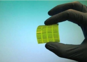
While memory devices are becoming progressively more flexible, their ease of fabrication and integration in low performance applications have been generally been treated as being of secondary importance. But now, thanks to new work, this is about to change. In a new article, they present a proof of concept, using resistive memory that now paves the way for mass-producing printable electronics.
Memory devices -- as a subset of electronic functions that includes logic, sensors and displays -- have undergone an exponential increase in integration and performance known as Moore's Law. In parallel, our daily lives increasingly involve an assortment of relatively low-performance electronic functions implemented in computer chips on credit cards, in-home appliances, and even smart tags on consumer products.
While memory devices are becoming progressively more flexible, their ease of fabrication and integration in low performance applications have been generally been treated as being of secondary importance. But now, thanks to the work of a group of researchers at Munich University of Applied Sciences in Germany and INRS-EMT in Canada, this is about to change.
Additive manufacturing, perhaps best known because of 3-D printing, allows for a streamlined process flow -- eliminating complex lithography and material removal steps at the detriment of feature size, which is in many cases not critical for memory devices in less computationally demanding uses.
Inkjet printing is a common office technology that competes with laser printing. It offers the added benefit of a straightforward transfer from inkjet to roll-to-roll printing. In an article appearing this week in Applied Physics Letters, from AIP Publishing, the group presents a proof of concept, using resistive memory (ReRAM) that now paves the way for mass-producing printable electronics.
The basic principle behind the group's ReRAM is simple. "In any kind of memory, the basic memory unit must be switchable between two states that represent one bit, or '0' or '1.' For ReRAM devices, these two states are defined by the resistance of the memory cell," explained Bernhard Huber, a doctoral student at INRS-EMT and working in the Laboratory for Microsystems Technology at Munich University of Applied Sciences.
For the conductive-bridge random access memory (CB-RAM) used by the group, "0" is "a high-resistance state represented by the high resistance of an insulating spin-on glass, which separates a conducting polymer electrode from a silver electrode," he continued. "The '1' is a low-resistance state, which is given by a metallic filament that grows into the spin-on glass and provides a reversible short-circuit between the two electrodes."
Rather than printing colors, "we use functional inks to deposit a capacitor structure -- conductor-insulator-conductor -- with materials that have already been deployed in cleanroom processes," Huber said. "This process is identical to that of an office inkjet printer, with an additional option of fine-tuning the droplet size and heating the target material."
The concept of CB-RAM is already well established and the group's leaders -- Andreas Ruediger of INRS-EMT in Canada and Christina Schindler of Munich University of Applied Sciences -- have previously worked on more conventional CB-RAM cells.
What's the significance of the group's work?
"We not only demonstrated that a complete additive (printing) process was possible but also that the performance parameters are comparable to cleanroom-fabricated devices," Schindler said. "The biggest technological appeal is the mechanical flexibility of our memory tiles, and the fact that all materials required for processing are commercially available."
"From our proof of concept, we're paving a road toward optimization," Schindler said. "Our biggest surprise was how little device performance depends on the fabrication process."
This enables extremely low-cost flexible electronics through printing processes. "Print-on-demand electronics are another large field of possible applications," Ruediger said. "At present, the main source of versatile electronics is field-programmable gate arrays that provide a reconfigurable circuitry that can be adopted for different purposes with predefined limitations."
Print-on-demand electronics show huge potential for small and inherently flexible lines of production and end-user products.
"Just imagine supermarkets printing their own smart tags or public transport providers customizing multifunctional tickets on demand. 'Wearables' that explicitly require flexible electronics may also benefit," Schindler said. The costs for such a printer, after optimization of the process steps, could drop to within the range of current inkjet printers.
Share on:


Testimonial
"Advertising in PCB007 Magazine has been a great way to showcase our bare board testers to the right audience. The I-Connect007 team makes the process smooth and professional. We’re proud to be featured in such a trusted publication."
Klaus Koziol - atgSuggested Items
Smartphone Production Rises 4% QoQ in 2Q25 as Inventory Adjustment Ends
09/12/2025 | TrendForceTrendForce’s latest investigations reveal that global smartphone production reached 300 million units in 2Q25, up 4% QoQ and 4.8% YoY, driven by seasonal demand and the recovery of brands such as Oppo and Transsion following inventory adjustments.
I-Connect007 Editor’s Choice: Five Must-Reads for the Week
09/12/2025 | Marcy LaRont, I-Connect007We may be post-Labor Day, but it is still hot-hot-hot here in the great state of Arizona—much like our news cycles, which have continued to snap, crackle, and pop with eye-raising headlines over this past week. In broader global tech news this week, AI and tariff-type restrictions continues to dominate with NVIDIA raising its voice against U.S. lawmakers pushing chip restrictions, ASML investing in a Dutch AI start-up company to the tune of $1.5 billion, and the UAE joining the ranks of the U.S. and China in embracing “open source” with their technology in hopes of accelerating their AI position.
Delta Electronics Posts 26.7% Growth in Sales Revenues for August
09/12/2025 | Delta ElectronicsDelta Electronics, Inc. announced its consolidated sales revenues for August 2025 totaled NT$47,860 million, a 26.7 percent increase as compared to NT$37,770 million for August 2024 and a 5.4 percent increase as compared to NT$45,397 million for July 2025.
Flex Named to TIME's World's Best Companies List for Third Consecutive Year
09/12/2025 | FlexFlex announced its inclusion on the TIME World's Best Companies 2025 list. This marks the third consecutive year the company was included in this prestigious ranking, which recognizes top-performing companies across the globe.
Direct Imaging System Market Size to Hit $4.30B by 2032, Driven by Increasing Demand for High-Precision PCB Manufacturing
09/11/2025 | Globe NewswireAccording to the SNS Insider, “The Direct Imaging System Market size was valued at $2.21 Billion in 2024 and is projected to reach $4.30 Billion by 2032, growing at a CAGR of 8.68% during 2025-2032.”