


 The Marketing Minute: Cracking the Code of Technical Marketing
 Trouble in Your Tank: Implementing Direct Metallization in Advanced Substrate Packaging


The Perfect Pattern to Trap Light
April 7, 2017 | A*STAREstimated reading time: 1 minute
Brighter LEDs and more efficient solar cells are two potential applications for A*STAR's research into lattice structures that can slow or trap light.
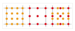
Harnessing wave energy by localizing it and suppressing its propagation through a medium is a powerful technique. Now, Alagappin Gandhi and Png Ching Eng Jason from the A*STAR Institute of High Performance Computing have calculated a design that localizes light in tiny loops, within a two-dimensional structure created by merging two lattices of slightly differing periodicities.
The new technique is not limited to light, and may enable the design of systems that can precisely control wave energy in any realm and at any scale — sound, thermal, water, or even matter waves such as in Bose-Einstein condensates.
For light-based devices the new insights could be used to build more efficient photonic components, said Gandhi.
“If you pattern the surface of an LED with merged lattices it will assist with getting the light out efficiently,” said Gandhi. “For a solar cell, however merged lattices will help light to enter better so that more energy can be harvested.”
The ability to create resonators in which light is localized on the surface of a device also has applications in quantum computing components based on light, such as defects in diamond.
Gandhi and Png designed the structures by superimposing lattices of small circular dielectric materials with periods in a simple ratio R:R-1 — for example one lattice is merged with another whose spacing is 4/3 as big, or 5/4, 6/5 etc.
“It creates a two-dimensional effect similar to beats between two waves of very close frequency,” Gandhi said. “Where there are antinodes the light is localized in the form of a closed path.”
Gandhi said the creation of a regular array of localized loops of light contrasted with Anderson Localization, which arises from randomness in a structure. “This is a systematic way of creating a large number of loops,” Gandhi said.
Gandhi and Png ran numerical simulations of the propagation of light in a range of wavelengths slightly below that of the lattice spacing, and calculated the energy band structure. They found that as R increased, there emerged a large number of energy bands whose light had a group velocity of zero, the signature of light localized within the crystal.
Gandhi said merged lattices would also provide a way for researchers to explore topological properties, such as protected edge modes.
Share on:


Testimonial
"We’re proud to call I-Connect007 a trusted partner. Their innovative approach and industry insight made our podcast collaboration a success by connecting us with the right audience and delivering real results."
Julia McCaffrey - NCAB GroupSuggested Items
Alternative Manufacturing, Inc. (AMI) Announces Commitment to Excellence in Industrial, Defense, Aerospace, Renewables, and Robotics Markets
09/16/2025 | Alternative Manufacturing, Inc.Alternative Manufacturing, Inc. (AMI), a 100% employee-owned contract manufacturer, proudly reaffirms its leadership in the electronics manufacturing services (EMS) industry with a continued commitment to delivering high-quality PCBAs and box builds across the industrial, defense, aerospace, renewable energy, and robotics markets.
Elementary Mr. Watson: Running the Signal Gauntlet
09/11/2025 | John Watson -- Column: Elementary, Mr. WatsonIf you’ve ever run a military obstacle course, you know it’s less “fun fitness challenge” and more “how can we inflict as much pain in the shortest time possible?” You start fresh—chest out, lungs full of confidence, thinking you might even look good doing this—and 10 seconds later, you’re questioning all your life choices.
Hitachi Unveils $1B U.S. Investment in Critical Grid Infrastructure
09/05/2025 | Hitachi EnergyHitachi Energy, a wholly owned subsidiary of Hitachi, Ltd., and global leader in electrification, today announced a historic investment of more than $1 billion USD to expand the production of critical electrical grid infrastructure in the United States.
Ferric Launches New Integrated Voltage Regulator for AI and High-Performance Processors
08/27/2025 | BUSINESS WIREFe1766 delivers an unprecedented 160 A in the industry’s smallest IVR footprint, redefining chip-level and system-level power delivery for the AI era.
Tigo Energy Initiates ‘Made in the USA’ Manufacturing Partnership With EG4 Electronics Share
08/27/2025 | BUSINESS WIRETigo Energy, Inc announced a manufacturing and marketing partnership with EG4 Electronics to produce Tigo optimized inverters and Module Level Power Electronics (MLPE) together with EG4 solar inverters in the United States of America.