


 The Marketing Minute: Cracking the Code of Technical Marketing
 Trouble in Your Tank: Implementing Direct Metallization in Advanced Substrate Packaging


Self-Assembling Polymers Provide Thin Nanowire Template
April 11, 2017 | Argonne National LaboratoryEstimated reading time: 4 minutes
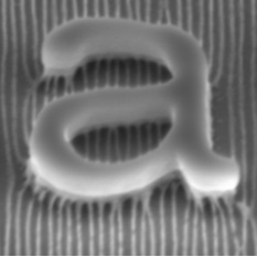
For the chips in our computers and smartphones to get faster and faster, their components – the circuits and wires through which signals flow – have to get smaller and smaller. The miniaturization of these wires has taken scientists on a journey almost to the atomic level. Recently, scientists have begun to address – and now to surmount – certain barriers in physics that have prevented them from making even smaller wires.
In a recent study, a team of researchers from the U.S. Department of Energy’s Argonne National Laboratory (DOE), the University of Chicago, and MIT has developed a new way to create some of the world’s thinnest wires, using a process that could enable mass manufacturing with standard types of equipment.
Templated assembly, or directed self-assembly, as it is known, represents an easier and more cost-effective way to make nanowires with widths below 10 nanometers (about 100 atoms thick).
The self-assembling materials are large molecules known as block copolymers. These block copolymers are the two-headed beasts of the chemical world – one end is water-loving, the other end is water-hating. Upon heating, they spontaneously form highly uniform structures at the molecular scale.
“A systems-level understanding of the template, topcoat, and self-assembling block copolymer is the key to the whole process.”
On their own, however, the block copolymers would form a pattern that looks like a fingerprint or a piece of brain coral – useless for the creation of functional nanowires. The key to changing that pattern to something more ordered is the use of the chemically patterned templates.
Past approaches to making tiny ordered nanostructures used expensive specialized optics to direct extreme wavelengths of light or electron beams to write patterns line-by-line. The new approach involves creating a chemical pattern as a template using these same tools at relatively low resolution, and then filling in the template to fabricate high-resolution patterns using a self-assembling material.
For very high-resolution block copolymer systems, a “topcoat” is often added during the process. This topcoat constrains the way the block copolymers self-assemble, forcing them into a regular, ordered structure perpendicular to the surface they are grown on.
“Think of it like baking a cake,” said Argonne nanoscientist Leonidas Ocola, a co-author of the study. “Without a mold for the cake, it can bake in a shape you don’t want it to bake. Having the mold gives it that shape that you want. The mold creates boundary conditions needed to define the shape you want.”
“The topcoat and underlying lithographic pattern work together to guide the formation of the nanostructure and provide the morphology we want,” he added.
Although self-assembling materials in nanomanufacturing have been known for quite a while, using block copolymers with the topcoat enables patterns for dense arrays of tiny wires.
“A systems-level understanding of the template, topcoat and self-assembling block copolymer is the key to the whole process – you need to find a way to induce the block copolymer film to assembly into desired architectures for manufacturing, and be able to transfer the pattern of the block copolymer into the actual device materials, such as semiconducting silicon wires or conducting copper wires,” said Paul Nealey, Brady W. Dougan Professor in Molecular Engineering at the Institute for Molecular Engineering at the University of Chicago and another author of the study.
Because the topcoat polymer layer does not need to be removed prior to pattern transfer steps, and additional layers can be patterned on top of the topcoat, the system can be used to build up many kinds of complex patterns, as would be needed for the interconnections of a microchip.
Most microchip manufacturing facilities use existing lithographic methods, and the chemical vapor deposition process used to create the topcoat is itself a well-understood additional step that could be added relatively easily. Thus, implementing the new method could be much more straightforward than other proposed methods of making finer lines.
With the new method, “you wouldn’t need to change all those machines,” said co-author Karen Gleason, MIT associate provost and Alexander and I. Michael Kasser Professor of Chemical Engineering. “And everything that’s involved are well-known materials.”
The new findings are reported in a Mar. 27 article in Nature Nanotechnology entitled, “Sub-10-nm patterning via directed self-assembly of block copolymer films with a vapour-phase deposited topcoat.” X-ray scattering experiments and electron-beam lithography were performed at Argonne’s Advanced Photon Source and Center for Nanoscale Materials, both DOE Office of Science User Facilities.
The work was also supported by the National Science Foundation and the U.S. Army Research Office, through MIT’s Institute for Soldier Nanotechnologies.
About Argonne National Laboratory
Argonne National Laboratory seeks solutions to pressing national problems in science and technology. The nation's first national laboratory, Argonne conducts leading-edge basic and applied scientific research in virtually every scientific discipline. Argonne researchers work closely with researchers from hundreds of companies, universities, and federal, state and municipal agencies to help them solve their specific problems, advance America's scientific leadership and prepare the nation for a better future. With employees from more than 60 nations, Argonne is managed by UChicago Argonne, LLC for the U.S. Department of Energy's Office of Science.
Share on:


Testimonial
"The I-Connect007 team is outstanding—kind, responsive, and a true marketing partner. Their design team created fresh, eye-catching ads, and their editorial support polished our content to let our brand shine. Thank you all! "
Sweeney Ng - CEE PCBSuggested Items
Trouble in Your Tank: Implementing Direct Metallization in Advanced Substrate Packaging
09/15/2025 | Michael Carano -- Column: Trouble in Your TankDirect metallization systems based on conductive graphite are gaining popularity throughout the world. The environmental and productivity gains achievable with this process are outstanding. Direct metallization reduces the costs of compliance, waste treatment, and legal issues related to chemical exposure. A graphite-based direct plate system has been devised to address these needs.
Closing the Loop on PCB Etching Waste
09/09/2025 | Shawn Stone, IECAs the PCB industry continues its push toward greener, more cost-efficient operations, Sigma Engineering’s Mecer System offers a comprehensive solution to two of the industry’s most persistent pain points: etchant consumption and rinse water waste. Designed as a modular, fully automated platform, the Mecer System regenerates spent copper etchants—both alkaline and acidic—and simultaneously recycles rinse water, transforming a traditionally linear chemical process into a closed-loop system.
Driving Innovation: Depth Routing Processes—Achieving Unparalleled Precision in Complex PCBs
09/08/2025 | Kurt Palmer -- Column: Driving InnovationIn PCB manufacturing, the demand for increasingly complex and miniaturized designs continually pushes the boundaries of traditional fabrication methods, including depth routing. Success in these applications demands not only on robust machinery but also sophisticated control functions. PCB manufacturers rely on advanced machine features and process methodologies to meet their precise depth routing goals. Here, I’ll explore some crucial functions that empower manufacturers to master complex depth routing challenges.
Trouble in Your Tank: Minimizing Small-via Defects for High-reliability PCBs
08/27/2025 | Michael Carano -- Column: Trouble in Your TankTo quote the comedian Stephen Wright, “If at first you don’t succeed, then skydiving is not for you.” That can be the battle cry when you find that only small-diameter vias are exhibiting voids. Why are small holes more prone to voids than larger vias when processed through electroless copper? There are several reasons.
The Government Circuit: Navigating New Trade Headwinds and New Partnerships
08/25/2025 | Chris Mitchell -- Column: The Government CircuitAs global trade winds continue to howl, the electronics manufacturing industry finds itself at a critical juncture. After months of warnings, the U.S. Government has implemented a broad array of tariff increases, with fresh duties hitting copper-based products, semiconductors, and imports from many nations. On the positive side, tentative trade agreements with Europe, China, Japan, and other nations are providing at least some clarity and counterbalance.