


 The Marketing Minute: Cracking the Code of Technical Marketing
 Trouble in Your Tank: Implementing Direct Metallization in Advanced Substrate Packaging


Method Improves Semiconductor Fiber Optics, Paves Way for Developing Devices
April 12, 2017 | Pennsylvania State UniversityEstimated reading time: 3 minutes
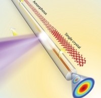
A new method to improve semiconductor fiber optics may lead to a material structure that might one day revolutionize the global transmission of data, according to an interdisciplinary team of researchers.
Researchers are working with semiconductor optical fibers, which hold significant advantages over silica-based fiber optics, the current technology used for transmitting nearly all digital data. Silica — glass — fibers can only transmit electronic data converted to light data. This requires external electronic devices that are expensive and consume enormous amounts of electricity. Semiconductor fibers, however, can transmit both light and electronic data and might also be able to complete the conversion from electrical to optical data on the fly during transmission, improving delivery speed.
Think of these conversions as exit ramps on the information superhighway, said Venkatraman Gopalan, professor of materials science and engineering, Penn State. The fewer the exits the data takes, the faster the information travels. Call it "fly-by optoelectronics," he said.
In 2006, researchers, led by John Badding, professor of chemistry, physics, and materials science and engineering, first developed silicon fibers by embedding silicon and other semiconductor materials into silica-fiber capillaries. The fibers, comprised of a series of crystals, were limited in their ability to transmit data because imperfections, such as grain boundaries at the surfaces where the many crystals within the fiber core bonded together, forced portions of the light to scatter, disrupting the transmission.
A method designed by Xiaoyu Ji, doctoral candidate in materials science and engineering, improves on the polycrystalline core of the fiber by melting a high-purity amorphous silicon core deposited inside a 1.7-micron inner-diameter glass capillary using a scanning laser, allowing for formation of silicon single crystals that were more than 2,000 times as long as they were thick. This method transforms the core from a polycrystal with many imperfections to a single crystal with few imperfections that transmits light much more efficiently.
That process, detailed in a trio of articles published in ACS Photonics, Advanced Optical Materials, and Applied Physics Letters early this year, demonstrates a new methodology to improve data transfer by eliminating imperfections in the fiber core that can be made of various materials. Gopalan said equipment constraints kept the crystals from being longer.
Because of the ultra-small core, Ji was able to melt and refine the crystal structure of the core material at temperatures of about 750 to 930 degrees Fahrenheit, lower than a typical fiber-drawing process for silicon core fibers. The lower temperatures and the short heating time that can be controlled by the laser power and the laser scanning speed also prevented the silica capillary, which has different thermal properties, from softening and contaminating the core.
"High purity is fundamentally important for high performance when dealing with materials designated for optical or electrical use," said Ji.
The important takeaway, said Gopalan, is that this new method lays out the methodology for how a host of materials can be embedded into fiber optics and how voids and imperfections can be reduced to increase light-transfer efficiency, necessary steps to advancing the science from its infancy.
"Glass technology has taken us this far," said Gopalan. "The ambitious idea that Badding and my group had about 10 years ago was that glass is great, but can we do more by using the numerous electronically and optically active materials other than plain glass. That's when we began trying to embed semiconductors into glass fiber."
Like fiber-optic cable, which took decades to become a reliable data-delivery device, decades of work likely remains to create commercially viable, semiconductor fiber networks. It took 10 years for researchers to reach polycrystalline fibers to specifications that are far better, but are still not competitive with traditional fiber-optic cable.
"Xiaoyu has been able to start from nicely deposited amorphous silicon and germanium core and use a laser to crystallize them, so that the whole semiconductor fiber core is one nice single crystal with no boundaries," said Gopalan. "This improved light and electronic transfer. Now we can make some real devices, not just for communications, but also for endoscopy, imaging, fiber lasers and many more."
Gopalan said he is not only in the business of creating commercially viable materials. He is interested in dreaming big and taking the long view on new technologies. Perhaps one day, every new home constructed might have a semiconductor fiber, bringing faster internet to it.
"This is why we got into this in the first place," said Gopalan. "Badding's group was able to figure out how to put silicon and germanium and metals and other semiconductors into the fiber, and this method improves on that."
The Penn State Materials Research Science and Engineering Center for Nanoscale Science funded this research.
Share on:


Testimonial
"In a year when every marketing dollar mattered, I chose to keep I-Connect007 in our 2025 plan. Their commitment to high-quality, insightful content aligns with Koh Young’s values and helps readers navigate a changing industry. "
Brent Fischthal - Koh YoungSuggested Items
Curing and Verification in PCB Shadow Areas
09/17/2025 | Doug Katze, DymaxDesign engineers know a simple truth that often complicates electronics manufacturing: Light doesn’t go around corners. In densely populated PCBs, adhesives and coatings often fail to fully cure in shadowed regions created by tall ICs, connectors, relays, and tight housings.
Marcy’s Musings: Advancing the Advanced Materials Discussion
09/17/2025 | Marcy LaRont -- Column: Marcy's MusingsAs the industry’s most trusted global source of original content about the electronics supply chain, we continually ask you about your concerns, what you care about, and what you most want to learn about. Your responses are insightful and valuable. Thank you for caring enough to provide useful feedback and engage in dialogue.
September 2025 PCB007 Magazine: The Future of Advanced Materials
09/16/2025 | I-Connect007 Editorial TeamMoore’s Law is no more, and the advanced material solutions being developed to grapple with this reality are surprising, stunning, and perhaps a bit daunting. Buckle up for a dive into advanced materials and a glimpse into the next chapters of electronics manufacturing.
I-Connect007 Launches Advanced Electronics Packaging Digest
09/15/2025 | I-Connect007I-Connect007 is pleased to announce the launch of Advanced Electronics Packaging Digest (AEPD), a new monthly digital newsletter dedicated to one of the most critical and rapidly evolving areas of electronics manufacturing: advanced packaging at the interconnect level.
Panasonic Industry will Double the Production Capacity of MEGTRON Multi-layer Circuit Board Materials Over the Next Five Years
09/15/2025 | Panasonic Industry Co., Ltd.Panasonic Industry Co., Ltd., a Panasonic Group company, announced plans for a major expansion of its global production capacity for MEGTRON multi-layer circuit board materials today. The company plans to double its production over the next five years to meet growing demand in the AI server and ICT infrastructure markets.