


 The Marketing Minute: Cracking the Code of Technical Marketing
 Trouble in Your Tank: Implementing Direct Metallization in Advanced Substrate Packaging


Novel Nanotube Structure Strengthens Thin Films for Flexible Electronics
April 24, 2017 | University of Illinois Urbana-ChampaignEstimated reading time: 3 minutes
Reflecting the structure of composites found in nature and the ancient world, researchers at the University of Illinois at Urbana-Champaign have synthesized thin carbon nanotube (CNT) textiles, that exhibit both high electrical conductivity and a level of toughness that is about fifty times higher than copper films, currently used in electronics.
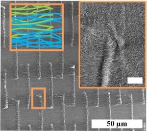
Scanning Electron Microscope Images of architectured carbon nanotube (CNT) textile made at Illinois. Colored schematic shows the architecture of self-weaved CNTs, and the inset shows a high resolution SEM of the inter-diffusion of CNT among the different patches due to capillary splicing.
“The structural robustness of thin metal films has significant importance for the reliable operation of smart skin and flexible electronics including biological and structural health monitoring sensors,” explained Sameh Tawfick, an assistant professor of mechanical science and engineering at Illinois. “Aligned carbon nanotube sheets are suitable for a wide range of application spanning the micro- to the macro-scales including Micro-Electro-Mechanical Systems (MEMS), supercapacitor electrodes, electrical cables, artificial muscles, and multi-functional composites.
“To our knowledge, this is the first study to apply the principles of fracture mechanics to design and study the toughness nano-architectured CNT textiles. The theoretical framework of fracture mechanics is shown to be very robust for a variety of linear and non-linear materials.”
Carbon nanotubes, which have been around since the early nineties, have been hailed as a “wonder material” for numerous nanotechnology applications, and rightly so. These tiny cylindrical structures made from wrapped graphene sheets have diameter of a few nanometers—about 1000 times thinner than a human hair, yet, a single carbon nanotube is stronger than steel and carbon fibers, more conductive than copper, and lighter than aluminum.
However, it has proven really difficult to construct materials, such as fabrics or films that demonstrate these properties on centimeter or meter scales. The challenge stems from the difficulty of assembling and weaving CNTs since they are so small, and their geometry is very hard to control.
“The study of the fracture energy of CNT textiles led us to design these extremely tough films,” stated Yue Liang, a former graduate student with the Kinetic Materials Research group and lead author of the paper, “Tough Nano-Architectured Conductive Textile Made by Capillary Splicing of Carbon Nanotubes,” appearing in Advanced Engineering Materials. To our knowledge, this is the first study of the fracture energy of CNT textiles.
Beginning with catalyst deposited on a silicon oxide substrate, vertically aligned carbon nanotubes were synthesized via chemical vapor deposition in the form of parallel lines of 5 µm width, 10 μm length, and 20–60 μm heights.
Example of stress-strain curve resulting from mechanical testing of carbon nanotube textile. The bottom chart shows the ability of the researchers to tune the mechanical behavior, namely strength (maximum force to breakage) and modulus (resistance to stretching) by varying the textile architecture.
“The staggered catalyst pattern is inspired by the brick and mortar design motif commonly seen in tough natural materials such as bone, nacre, the glass sea sponge, and bamboo,” Liang added. “Looking for ways to staple the CNTs together, we were inspired by the splicing process developed by ancient Egyptians 5,000 years ago to make linen textiles. We tried several mechanical approaches including micro-rolling and simple mechanical compression to simultaneously re-orient the nanotubes, then, finally, we used the self-driven capillary forces to staple the CNTs together.”
“This work combines careful synthesis, and delicate experimentation and modeling,” Tawfick said. “Flexible electronics are subject to repeated bending and stretching, which could cause their mechanical failure. This new CNT textile, with simple flexible encapsulation in an elastomer matrix, can be used in smart textiles, smart skins, and a variety of flexible electronics. Owing to their extremely high toughness, they represent an attractive material, which can replace thin metal films to enhance device reliability.”
Share on:


Testimonial
"Our marketing partnership with I-Connect007 is already delivering. Just a day after our press release went live, we received a direct inquiry about our updated products!"
Rachael Temple - AlltematedSuggested Items
Trouble in Your Tank: Implementing Direct Metallization in Advanced Substrate Packaging
09/15/2025 | Michael Carano -- Column: Trouble in Your TankDirect metallization systems based on conductive graphite are gaining popularity throughout the world. The environmental and productivity gains achievable with this process are outstanding. Direct metallization reduces the costs of compliance, waste treatment, and legal issues related to chemical exposure. A graphite-based direct plate system has been devised to address these needs.
Closing the Loop on PCB Etching Waste
09/09/2025 | Shawn Stone, IECAs the PCB industry continues its push toward greener, more cost-efficient operations, Sigma Engineering’s Mecer System offers a comprehensive solution to two of the industry’s most persistent pain points: etchant consumption and rinse water waste. Designed as a modular, fully automated platform, the Mecer System regenerates spent copper etchants—both alkaline and acidic—and simultaneously recycles rinse water, transforming a traditionally linear chemical process into a closed-loop system.
Driving Innovation: Depth Routing Processes—Achieving Unparalleled Precision in Complex PCBs
09/08/2025 | Kurt Palmer -- Column: Driving InnovationIn PCB manufacturing, the demand for increasingly complex and miniaturized designs continually pushes the boundaries of traditional fabrication methods, including depth routing. Success in these applications demands not only on robust machinery but also sophisticated control functions. PCB manufacturers rely on advanced machine features and process methodologies to meet their precise depth routing goals. Here, I’ll explore some crucial functions that empower manufacturers to master complex depth routing challenges.
Trouble in Your Tank: Minimizing Small-via Defects for High-reliability PCBs
08/27/2025 | Michael Carano -- Column: Trouble in Your TankTo quote the comedian Stephen Wright, “If at first you don’t succeed, then skydiving is not for you.” That can be the battle cry when you find that only small-diameter vias are exhibiting voids. Why are small holes more prone to voids than larger vias when processed through electroless copper? There are several reasons.
The Government Circuit: Navigating New Trade Headwinds and New Partnerships
08/25/2025 | Chris Mitchell -- Column: The Government CircuitAs global trade winds continue to howl, the electronics manufacturing industry finds itself at a critical juncture. After months of warnings, the U.S. Government has implemented a broad array of tariff increases, with fresh duties hitting copper-based products, semiconductors, and imports from many nations. On the positive side, tentative trade agreements with Europe, China, Japan, and other nations are providing at least some clarity and counterbalance.