


 The Marketing Minute: Cracking the Code of Technical Marketing
 Trouble in Your Tank: Implementing Direct Metallization in Advanced Substrate Packaging


Supercomputing: Probing the Future
April 26, 2017 | NISTEstimated reading time: 3 minutes
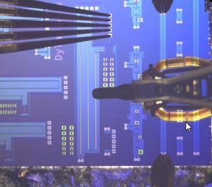
NIST scientists have developed a novel automated probe system for evaluating the performance of computer components designed to run 100 times faster than today’s best supercomputers and consume as little as 1/1000th the energy.
That range of performance, as envisioned in the National Strategic Computing Initiative (NSCI), is the overarching goal of many private-sector and federal programs studying different technologies and platforms. One of those is the Cryogenic Computing Complexity (C3) program, supported by the Intelligence Advanced Research Projects Activity (link is external) agency (IARPA). Its aim is to enable a new generation of low-power superconducting supercomputers that operate at liquid-helium temperatures and use ultra-fast switching of microscopic circuit elements called Josephson junctions.
No one yet knows the best way (or ways) to do that. Under the terms of the C3 program, each of three different industry participants creates prototype memory and logic units designed to perform within program parameters. The job of independently testing those devices falls to NIST.
“What they want NIST to do is verify that those devices perform as the makers say they do,” says William Rippard, leader of NIST’s Spin Electronics Group, which is testing memory components. “That means that we have to be able to measure uncommonly faint signals on unusually fast time scales. Both have required us to develop new measurement capabilities. The new probe system is a major part of that effort.”
NIST is responsible for characterizing each individual device (typically 100 nm to 1 µm) in each chip (typically 5 mm to 10 mm in size) and its subcomponents at liquid helium temperature (4 kelvin). For this they employ a cryostat that has a temperature instability of only 50 millikelvin, inside of which is a NIST-designed three-axis manipulator guided by an optical feedback system to probe specific points. But the researchers also test the same devices at room temperature to look for correlations in properties across a span of about 300 K. This will allow room-temperature testing of devices to provide quantitative predictive behavior at 4 K.
Because a circuit might contain large arrays of 10,000 or more Josephson junctions, testing each of them individually is a daunting task. The NIST scientists developed a fully automated system capable of exactly positioning the probe tip using optical feedback from a camera looking down at the surface of the chip at 4 K. That arrangement allows the probe tip to move over the device in precisely incremented steps.
Another challenge is the speed involved. The superconducting circuits operate on time scales of picoseconds -- a millionth of a millionth of a second. “In a typical setup, you have maybe two meters of cable that runs between the device you’re testing and the instrumentation,” Rippard says. “When a picosecond pulse travels through that much cable, it gets attenuated and spread out. What started as a really sharp signal is stretched out until it looks like a bell curve.”
To circumvent that problem, the group is devising specialized circuits that will allow them to amplify the signal only centimeters away from the chip that produced it. Conversely, to send ultra-short signals to the chip, they use a femtosecond laser (firing at pulse of light 0.2 picoseconds in duration) and convert the optical signal to an electric pulse in the range of a few picoseconds.
The probe electrodes can be replaced with highly responsive sensors that measure a 2D pattern of magnetic activity across the chip. The group built a system that uses a read-write head from a hard disk drive to measure those fields, and a much more sensitive replacement is in development. Because each minuscule trace that carries moving electrons generates a magnetic field, the magnetic data constitute a map of current flow revealing buried electrical layers.
The magnetic measurements will also locate the vortices -- small eddies of current -- that form under certain conditions in superconducting materials, and determine whether the vortices are immobile (“pinned”) in a single location or can move around the superconducting circuit and thereby generate resistance to supercurrent flow.
NIST’s role in C3 also contributes to an agency-wide initiative intended to develop the broader measurement capabilities needed to test and evaluate components for future high-performance computing. The NSCI names NIST as a “foundational research and development” agency with the mission of focusing on “measurement science to support future computing technologies.”
"This partnership with IARPA on the C3 supercomputing program,” says Bob Hickernell, Chief of NIST’s Quantum Electromagnetics Division, “combines the expertise of industry leaders in both cryogenic memory and logic circuitry development together with NIST's expertise in superconducting electronics and magnetics measurements at ultra-low temperatures to accelerate progress that promises high impact in areas including biomedical understanding and treatments, advanced materials development, and high-accuracy weather forecasting."
Share on:


Testimonial
"We’re proud to call I-Connect007 a trusted partner. Their innovative approach and industry insight made our podcast collaboration a success by connecting us with the right audience and delivering real results."
Julia McCaffrey - NCAB GroupSuggested Items
India’s Aerospace and Defence Engineered for Power, Driven by Electronics
09/16/2025 | Gaurab Majumdar, Global Electronics AssociationWith a defence budget of $82.05 billion (2025–26) and a massive $223 billion earmarked for aerospace and defence spending over the next decade, India is rapidly positioning itself as a major player in the global defence and aerospace market.
I-Connect007 Launches Advanced Electronics Packaging Digest
09/15/2025 | I-Connect007I-Connect007 is pleased to announce the launch of Advanced Electronics Packaging Digest (AEPD), a new monthly digital newsletter dedicated to one of the most critical and rapidly evolving areas of electronics manufacturing: advanced packaging at the interconnect level.
VIDEOTON EAS's Bulgarian Subsidiary Expands Into Automotive Products
09/15/2025 | VideotonVEAS Bulgaria, engaged in electronics manufacturing, has joined the ranks of VIDEOTON companies authorized to produce automotive products.
Variosystems Strengthens North American Presence with Southlake Relaunch 2025
09/15/2025 | VariosystemsVariosystems celebrated the relaunch of its U.S. facility in Southlake, Texas. After months of redesign and reorganization, the opening marked more than just the return to a modernized production site—it was a moment to reconnect with our teams, partners, and the local community.
Hanwha Aerospace to Collaborate with BAE Systems on Advanced Anti-jamming GPS for Guided Missiles
09/15/2025 | HanwhaHanwha Aerospace has signed a contract with BAE Systems to integrate next-generation, anti-jamming Global Positioning System (GPS) technology into Hanwha Aerospace’s Deep Strike Capability precision-guided weapon system.