


 The Marketing Minute: Cracking the Code of Technical Marketing
 Trouble in Your Tank: Implementing Direct Metallization in Advanced Substrate Packaging


Berkeley Lab Scientists Discover New Atomically Layered, Thin Magnet
April 27, 2017 | DOE/Lawrence Berkeley National LaboratoryEstimated reading time: 4 minutes
It may not seem like a material as thin as an atom could hide any surprises, but a research team led by scientists at the Department of Energy’s Lawrence Berkeley National Laboratory (Berkeley Lab) discovered an unexpected magnetic property in a two-dimensional material.
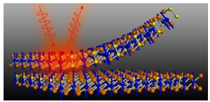
Illustration of Kerr effect used to detect magnetization through the rotation of polarized light when it interacts with electron spins in a material. Shown are layers of chromium germanium telluride (CGT). Tellurium atoms are orange, germanium is yellow, and chromium is blue. (Credit: Zhenglu Li/Berkeley Lab)
The scientists found that a 2-D van der Waals crystal, part of a class of material whose atomically thin layers can be peeled off one by one with adhesive tape, possessed an intrinsic ferromagnetism.
The discovery, published April 26 in the journal Nature, could have major implications for a wide range of applications that rely upon ferromagnetic materials, such as nanoscale memory, spintronic devices, and magnetic sensors.
“This is an exciting discovery,” said study principal investigator Xiang Zhang, senior faculty scientist at Berkeley Lab’s Materials Sciences Division and UC Berkeley professor. “This experiment presents smoking-gun evidence for an atomically thin—and atomically flat—magnet, which surprised many people. It opens the door for exploring fundamental spin physics and spintronic applications at low dimensions.”
The study tackles a long-standing issue in quantum physics about whether magnetism would survive when materials shrink down to two dimensions. For half a century, the Mermin-Wagner theorem has addressed this question by stating that if 2-D materials lack magnetic anisotropy, a directional alignment of electron spins in the material, there may be no magnetic order.
“Interestingly, we found that magnetic anisotropy is an inherent property in the 2-D material we studied, and because of this characteristic, we were able to detect the intrinsic ferromagnetism,” said study lead author Cheng Gong, a postdoctoral researcher in Zhang’s lab.
Van der Waals forces, named after a Dutch scientist, refers to intermolecular forces of attraction that do not arise from the typical covalent or ionic bonds that keep molecules intact. These quantum forces are used by geckos as they effortlessly scamper along walls and ceilings.
Van der Waals crystals describe materials in which the 2-D layers are not connected to each other via traditional bonds, allowing them to be easily exfoliated with tape. Research on graphene, the most well-known van der Waals material, earned the Nobel Prize in physics in 2010.
“It’s like the pages of a book,” said Gong. “The pages can be stacked on top of each other, but the forces linking one page to another is much weaker than the in-plane forces that keep a single sheet intact.”
Gong estimates that for this study, he peeled off more than 3,000 flakes of chromium germanium telluride (Cr2Ge2Te6, or CGT). While CGT has existed as a bulk material for decades, the researchers say the 2-D flakes could represent an exciting new family of 2-D van der Waals crystal.
“CGT is also a semiconductor, and the ferromagnetism is intrinsic,” said co-senior author Jing Xia, UC Irvine associate professor of physics and astronomy. “That makes it cleaner for applications in memory and spintronics.”
The researchers detected the magnetization from atomically thin materials using a technique called magneto-optic Kerr effect. The method involves the super-sensitive detection of the rotation of linearly polarized light when it interacts with electron spins in the material.
The key to one of the study’s more surprising findings is that the magnetic anisotropy was very small in the CGT material. That enabled researchers to easily control the temperature at which the material loses its ferromagnetism, known as the transition or Curie temperature.
“This is a significant discovery,” said Gong, “People believe that the Curie temperature is an inherent property of a magnetic material and cannot be changed. Our study shows that it can.”
The researchers showed that they could control the transition temperature of the CGT flake using surprisingly small magnetic fields of 0.3 tesla or less.
“Thin films of metals like iron, cobalt, and nickel, unlike 2-D van der Waals materials, are structurally imperfect and susceptible to various disturbances, which contribute to a huge and unpredictable spurious anisotropy,” said Gong. “In contrast, the highly crystalline and uniformly flat 2-D CGT, together with its small intrinsic anisotropy, allows small external magnetic fields to effectively engineer the anisotropy, enabling an unprecedented magnetic field control of ferromagnetic transition temperatures.”
The study authors also pointed out that a striking feature of van der Waals crystals is that they can be easily combined with dissimilar materials without restrictions based on structural or chemical compatibility.
“The opportunities to combine different materials to develop new functionalities are appealing,” said co-senior author Steven Louie, senior faculty scientist at Berkeley Lab’s Materials Sciences Division and UC Berkeley professor of physics. “This offers a huge amount of flexibility in designing artificial structures for diverse magneto-electric and magneto-optical applications.”
Other senior collaborators on this work include Zi Qiang Qiu at Berkeley Lab and UC Berkeley; and Robert Cava at Princeton University.
This work was primarily supported by DOE’s Office of Science.
Share on:


Testimonial
"We’re proud to call I-Connect007 a trusted partner. Their innovative approach and industry insight made our podcast collaboration a success by connecting us with the right audience and delivering real results."
Julia McCaffrey - NCAB GroupSuggested Items
Curing and Verification in PCB Shadow Areas
09/17/2025 | Doug Katze, DymaxDesign engineers know a simple truth that often complicates electronics manufacturing: Light doesn’t go around corners. In densely populated PCBs, adhesives and coatings often fail to fully cure in shadowed regions created by tall ICs, connectors, relays, and tight housings.
Marcy’s Musings: Advancing the Advanced Materials Discussion
09/17/2025 | Marcy LaRont -- Column: Marcy's MusingsAs the industry’s most trusted global source of original content about the electronics supply chain, we continually ask you about your concerns, what you care about, and what you most want to learn about. Your responses are insightful and valuable. Thank you for caring enough to provide useful feedback and engage in dialogue.
September 2025 PCB007 Magazine: The Future of Advanced Materials
09/16/2025 | I-Connect007 Editorial TeamMoore’s Law is no more, and the advanced material solutions being developed to grapple with this reality are surprising, stunning, and perhaps a bit daunting. Buckle up for a dive into advanced materials and a glimpse into the next chapters of electronics manufacturing.
I-Connect007 Launches Advanced Electronics Packaging Digest
09/15/2025 | I-Connect007I-Connect007 is pleased to announce the launch of Advanced Electronics Packaging Digest (AEPD), a new monthly digital newsletter dedicated to one of the most critical and rapidly evolving areas of electronics manufacturing: advanced packaging at the interconnect level.
Panasonic Industry will Double the Production Capacity of MEGTRON Multi-layer Circuit Board Materials Over the Next Five Years
09/15/2025 | Panasonic Industry Co., Ltd.Panasonic Industry Co., Ltd., a Panasonic Group company, announced plans for a major expansion of its global production capacity for MEGTRON multi-layer circuit board materials today. The company plans to double its production over the next five years to meet growing demand in the AI server and ICT infrastructure markets.