


 The Marketing Minute: Cracking the Code of Technical Marketing
 Trouble in Your Tank: Implementing Direct Metallization in Advanced Substrate Packaging


Diamond Quantum Sensor Reveals How Current Flows in Next Generation Materials
April 27, 2017 | University of MelbourneEstimated reading time: 3 minutes
Researchers at the University of Melbourne are the first in the world to image how electrons move in two-dimensional graphene, a boost to the development of next-generation electronics.
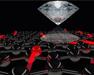
Artist's impression of a diamond quantum sensor. The 'spotlight' represents light passing through the diamond defect and detecting the movement of electrons. Electrons are shown as red spheres, trailed by red threads that reveal their path through graphene (a single layer of carbon atoms). David A. Broadway/cqc2t.org
Capable of imaging the behaviour of moving electrons in structures only one atom in thickness, the new technique overcomes significant limitations with existing methods for understanding electric currents in devices based on ultra-thin materials.
“Next-generation electronic devices based on ultra-thin materials, including quantum computers, will be especially vulnerable to contain minute cracks and defects that disrupt current flow,” said Professor Lloyd Hollenberg, Deputy Director of the Centre for Quantum Computation and Communication Technology (CQC2T) and Thomas Baker Chair at the University of Melbourne.
A team led by Hollenberg used a special quantum probe based on an atomic-sized ‘colour centre’ found only in diamonds to image the flow of electric currents in graphene. The technique could be used to understand electron behaviour in a variety of new technologies.
“The ability to see how electric currents are affected by these imperfections will allow researchers to improve the reliability and performance of existing and emerging technologies. We are very excited by this result, which enables us to reveal the microscopic behaviour of current in quantum computing devices, graphene and other 2D materials,” he said.
“Researchers at CQC2T have made great progress in atomic-scale fabrication of nanoelectronics in silicon for quantum computers. Like graphene sheets, these nanoelectronic structures are essentially one atom thick. The success of our new sensing technique means we have the potential to observe how electrons move in such structures and aid our future understanding of how quantum computers will operate.”
In addition to understanding nanoelectronics that control quantum computers, the technique could be used with 2D materials to develop next generation electronics, energy storage (batteries), flexible displays and bio-chemical sensors.
“Our technique is powerful yet relatively simple to implement, which means it could be adopted by researchers and engineers from a wide range of disciplines,” said lead author Dr Jean-Philippe Tetienne from CQC2T at the University of Melbourne.
“Using the magnetic field of moving electrons is an old idea in physics, but this is a novel implementation at the microscale with 21st Century applications.”
The work was a collaboration between diamond-based quantum sensing and graphene researchers. Their complementary expertise was crucial to overcoming technical issues with combining diamond and graphene.
“No one has been able to see what is happening with electric currents in graphene before,” said Nikolai Dontschuk, a graphene researcher at the University of Melbourne School of Physics.
“Building a device that combined graphene with the extremely sensitive nitrogen vacancy colour centre in diamond was challenging, but an important advantage of our approach is that it’s non-invasive and robust – we don’t disrupt the current by sensing it in this way,” he said.
Tetienne explained how the team was able to use diamond to successfully image the current.
“Our method is to shine a green laser on the diamond, and see red light arising from the colour centre’s response to an electron’s magnetic field,” he said.
“By analysing the intensity of the red light, we determine the magnetic field created by the electric current and are able to image it, and literally see the effect of material imperfections.”
The current-imaging results were published today in the prestigious Science Advances journal and are the culmination of a year’s work. The research is supported with funding from the Australian Research Council through the Centre of Excellence and Laureate Fellowship programs.
Share on:


Testimonial
"Advertising in PCB007 Magazine has been a great way to showcase our bare board testers to the right audience. The I-Connect007 team makes the process smooth and professional. We’re proud to be featured in such a trusted publication."
Klaus Koziol - atgSuggested Items
MEMS & Imaging Sensors Summit to Spotlight Sensing Revolution for Europe’s Leadership
09/11/2025 | SEMIIndustry experts will gather November 19-20 at the SEMI MEMS & Imaging Sensors Summit 2025 to explore the latest breakthroughs in AI-driven MEMS and imaging optimization, AR/VR technologies, and advanced sensor solutions for critical defence applications.
Direct Imaging System Market Size to Hit $4.30B by 2032, Driven by Increasing Demand for High-Precision PCB Manufacturing
09/11/2025 | Globe NewswireAccording to the SNS Insider, “The Direct Imaging System Market size was valued at $2.21 Billion in 2024 and is projected to reach $4.30 Billion by 2032, growing at a CAGR of 8.68% during 2025-2032.”
I-Connect007’s Editor’s Choice: Five Must-Reads for the Week
07/04/2025 | Marcy LaRont, I-Connect007For our industry, we have seen several bullish market announcements over the past few weeks, including one this week by IDC on the massive growth in the global server market. We’re also closely watching global trade and nearshoring. One good example of successful nearshoring is Rehm Thermal Systems, which celebrates its 10th anniversary in Mexico and the official opening of its new building in Guadalajara.
Driving Innovation: Direct Imaging vs. Conventional Exposure
07/01/2025 | Simon Khesin -- Column: Driving InnovationMy first camera used Kodak film. I even experimented with developing photos in the bathroom, though I usually dropped the film off at a Kodak center and received the prints two weeks later, only to discover that some images were out of focus or poorly framed. Today, every smartphone contains a high-quality camera capable of producing stunning images instantly.
United Electronics Corporation Advances Manufacturing Capabilities with Schmoll MDI-ST Imaging Equipment
06/24/2025 | United Electronics CorporationUnited Electronics Corporation has successfully installed the advanced Schmoll MDI-ST (XL) imaging equipment at their advanced printed circuit board facility. This significant technology investment represents a continued commitment to delivering superior products and maintaining their position as an industry leader in precision PCB manufacturing.