


 The Marketing Minute: Cracking the Code of Technical Marketing
 Trouble in Your Tank: Implementing Direct Metallization in Advanced Substrate Packaging


Unexpected Damage Found Rippling Through Promising Exotic Nanomaterials
April 28, 2017 | BNLEstimated reading time: 4 minutes
Some of the most promising and puzzling phenomena in physics play out on the nanoscale, where a billionth-of-a-meter shift can make or break perfect electrical conductivity.
Now, scientists have developed a new method to probe three-dimensional, atomic-scale intricacies and chemical compositions with unprecedented precision. The breakthrough technique—described February 6 in the journal Nano Letters—combines atomic-force microscopy with near-field spectroscopy to expose the surprising damage wreaked by even the most subtle forces.
“This is like granting sight to the blind,” said lead author Adrian Gozar of Yale University. “We can finally see the all-important variations that dictate functionality at this scale and better explore both cutting-edge electronics and fundamental questions that have persisted for decades.”
Scientists from Yale University, Harvard University, and the U.S. Department of Energy’s Brookhaven National Laboratory developed the technique to determine why a particular device fabrication technique—helium-ion beam lithography—failed to create the scalable, high-performing superconducting nanowires predicted by both theory and simulation.
In previous work, heavy ion beams were used to carve 10-nm-wide channels—some 10,000 times thinner than a human hair—through custom-made materials. However, the new study revealed beam-induced damage rippling out over 50 times that distance. At this scale, that difference was both imperceptible and functionally catastrophic.
“This directly addresses the challenge of quantum computing, for example, where companies including IBM and Google are exploring superconducting nanowires but need reliable synthesis and characterization,” said study coauthor and Brookhaven Lab physicist Ivan Bozovic.
Writing with ions
One promising design for high-temperature superconducting devices is alternating superconductor-insulator-superconductor (SIS) interfaces—or so-called Josephson junctions. These are theoretically easy to fabricate by direct beam writing, assuming sufficient precision can be achieved.
Helium-ion beam lithography (HIB) was a perfect candidate, proven recently in similar materials and well suited for swift and scalable production of superconducting nanowires and Josephson junctions.
“HIB lets us focus the particle beam to less than a single nanometer and effectively ‘write’ patterns to create superconducting interfaces,” said Nicholas Litombe, who led the HIB work under the guidance of Professor Jenny Hoffman of Harvard, a coauthor of this study. “We set out to shift that technique to another class of materials: LSCO thin films.”
The collaboration started with the painstaking assembly of perfect LSCO thin films—so named for their use of lanthanum, strontium, copper, and oxygen. Bozovic’s group at Brookhaven used a technique called atomic layer-by-layer molecular beam epitaxy, which can create atomically perfect superconducting films and heterostructures.
“I have a long-standing interest and specialization in using interphase physics to induce and understand high-temperature superconductivity,” Bozovic said. “HIB gives us an entirely new way to explore these materials on the nanoscale.”
Litombe carved the ultra-precise interface channels in Bozovic’s thin films. But the immediate results were discouraging: the anticipated superconductivity was entirely suppressed when current ran through wires narrower than a couple hundred nanometers.
“Our computer models and experimental results all looked excellent, but we knew there were hidden forces at work,” Litombe said. “We needed deeper insight into the material structure.”
Cryogenic lightning rod
Material composition and electronic properties can be pinpointed through the way they absorb and emit light—a longstanding field called spectroscopy. In the instance of superconductivity, this can distinguish between the “shiny” surface of a conductive metal versus the dullness of a current-breaking insulator.
The scientists turned to scanning near-field optical microscopy (SNOM) to examine the spectroscopic sheen on the HIB pathways. But this technique, which funnels light through a gilded glass capillary, has a resolution limit of about 100 nanometers—much too large to examine the nanoscale superconducting interfaces.
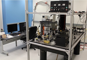
Fortunately, Gozar built a specialized instrument to radically increase the spectroscopic resolution. The machine, built entirely at Brookhaven Lab and now housed at Yale, combines SNOM with atomic force microscopy (AFM). Like a record player’s needle extracting sound from the texture of vinyl, an AFM needle travels over a material and reads the atomic topography.
“Here, the AFM needle acts like a lightning rod, channeling the SNOM light down to just tens of nanometers,” Gozar said. “We have simultaneous AFM topography and spectroscopic data on the deep chemical structures.”
Crucially, Gozar’s AFM-SNOM system also operates at the cryogenic temperatures required to test these materials—a capability only offered at a few laboratories in the world.
Widespread ruin
The novel technique revealed the unexpected and widespread damage left in the wake of the helium ions. Despite the 0.5-nanometer focus of the beam, its effects rattled atoms across a 500-nanometer spread and altered the structure enough to prevent superconductivity. For nanomaterial construction, this so-called lateral straggle is utterly untenable.
“Even the slightest nudge at this scale shatters the powerful phenomena we mean to exploit,” Litombe said. “High-temperature superconductivity can have a coherence distance of just a few atoms, so this lateral effect is devastating. We are, of course, still thrilled to explore the never-before-seen details.”
Added Bozovic, “In one sense, the whole result was negative. Our initial goal of creating nanometer-thick superconducting wires was not fully accomplished. But figuring out why has opened some truly exciting doors.”
The SNOM-AFM technique is readily applicable to fields such as plasmonics for display technology and the study of the mechanism behind high-temperature superconductivity.
“The nanoscale resolution and the tomographic capabilities of the instrument, put us on the cusp of uncovering new truths about nanoscale phenomena and the technology it empowers,” Gozar said.
This research was supported by the U.S. Department of Energy’s Office of Science and the Gordon and Betty Moore Foundation.
Brookhaven National Laboratory is supported by the Office of Science of the U.S. Department of Energy. The Office of Science is the single largest supporter of basic research in the physical sciences in the United States, and is working to address some of the most pressing challenges of our time. For more information, please visit science.energy.gov.
Share on:


Testimonial
"The I-Connect007 team is outstanding—kind, responsive, and a true marketing partner. Their design team created fresh, eye-catching ads, and their editorial support polished our content to let our brand shine. Thank you all! "
Sweeney Ng - CEE PCBSuggested Items
Trouble in Your Tank: Implementing Direct Metallization in Advanced Substrate Packaging
09/15/2025 | Michael Carano -- Column: Trouble in Your TankDirect metallization systems based on conductive graphite are gaining popularity throughout the world. The environmental and productivity gains achievable with this process are outstanding. Direct metallization reduces the costs of compliance, waste treatment, and legal issues related to chemical exposure. A graphite-based direct plate system has been devised to address these needs.
Closing the Loop on PCB Etching Waste
09/09/2025 | Shawn Stone, IECAs the PCB industry continues its push toward greener, more cost-efficient operations, Sigma Engineering’s Mecer System offers a comprehensive solution to two of the industry’s most persistent pain points: etchant consumption and rinse water waste. Designed as a modular, fully automated platform, the Mecer System regenerates spent copper etchants—both alkaline and acidic—and simultaneously recycles rinse water, transforming a traditionally linear chemical process into a closed-loop system.
Driving Innovation: Depth Routing Processes—Achieving Unparalleled Precision in Complex PCBs
09/08/2025 | Kurt Palmer -- Column: Driving InnovationIn PCB manufacturing, the demand for increasingly complex and miniaturized designs continually pushes the boundaries of traditional fabrication methods, including depth routing. Success in these applications demands not only on robust machinery but also sophisticated control functions. PCB manufacturers rely on advanced machine features and process methodologies to meet their precise depth routing goals. Here, I’ll explore some crucial functions that empower manufacturers to master complex depth routing challenges.
Trouble in Your Tank: Minimizing Small-via Defects for High-reliability PCBs
08/27/2025 | Michael Carano -- Column: Trouble in Your TankTo quote the comedian Stephen Wright, “If at first you don’t succeed, then skydiving is not for you.” That can be the battle cry when you find that only small-diameter vias are exhibiting voids. Why are small holes more prone to voids than larger vias when processed through electroless copper? There are several reasons.
The Government Circuit: Navigating New Trade Headwinds and New Partnerships
08/25/2025 | Chris Mitchell -- Column: The Government CircuitAs global trade winds continue to howl, the electronics manufacturing industry finds itself at a critical juncture. After months of warnings, the U.S. Government has implemented a broad array of tariff increases, with fresh duties hitting copper-based products, semiconductors, and imports from many nations. On the positive side, tentative trade agreements with Europe, China, Japan, and other nations are providing at least some clarity and counterbalance.