


 The Marketing Minute: Cracking the Code of Technical Marketing
 Trouble in Your Tank: Implementing Direct Metallization in Advanced Substrate Packaging


Scientists Set Record Resolution for Drawing at the One-Nanometer Length Scale
May 1, 2017 | BNLEstimated reading time: 4 minutes
The ability to pattern materials at ever-smaller sizes—using electron-beam lithography (EBL), in which an electron-sensitive material is exposed to a focused beam of electrons, as a primary method—is driving advances in nanotechnology. When the feature size of materials is reduced from the macroscale to the nanoscale, individual atoms and molecules can be manipulated to dramatically alter material properties, such as color, chemical reactivity, electrical conductivity, and light interactions.
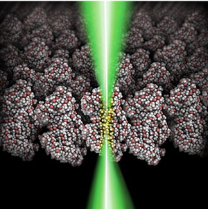
A schematic showing a focused electron beam (green) shining through a polymeric film (grey: carbon atoms; red: oxygen atoms; white: hydrogen atoms). The glowing area (yellow) indicates the molecular volume chemically modified by the focused electron beam.
In the ongoing quest to pattern materials with ever-smaller feature sizes, scientists at the Center for Functional Nanomaterials (CFN)—a U.S. Department of Energy (DOE) Office of Science User Facility at Brookhaven National Laboratory—have recently set a new record. Performing EBL with a scanning transmission electron microscope (STEM), they have patterned thin films of the polymer poly(methyl methacrylate), or PMMA, with individual features as small as one nanometer (nm), and with a spacing between features of 11 nm, yielding an areal density of nearly one trillion features per square centimeter. These record achievements are published in the April 18 online edition of Nano Letters.
“Our goal at CFN is to study how the optical, electrical, thermal, and other properties of materials change as their feature sizes get smaller,” said lead author Vitor Manfrinato, a research associate in CFN’s electron microscopy group who began the project as a CFN user while completing his doctoral work at MIT. “Until now, patterning materials at a single nanometer has not been possible in a controllable and efficient way.”
Commercial EBL instruments typically pattern materials at sizes between 10 and 20 nanometers. Techniques that can produce higher-resolution patterns require special conditions that either limit their practical utility or dramatically slow down the patterning process. Here, the scientists pushed the resolution limits of EBL by installing a pattern generator—an electronic system that precisely moves the electron beam over a sample to draw patterns designed with computer software—in one of CFN’s aberration-corrected STEMs, a specialized microscope that provides a focused electron beam at the atomic scale.
“We converted an imaging tool into a drawing tool that is capable of not only taking atomic-resolution images but also making atomic-resolution structures,” said coauthor Aaron Stein, a senior scientist in the electronic nanomaterials group at CFN.
Their measurements with this instrument show a nearly 200 percent reduction in feature size (from 5 to 1.7 nm) and 100 percent increase in areal pattern density (from 0.4 to 0.8 trillion dots per square centimeter, or from 16 to 11 nm spacing between features) over previous scientific reports.
The team’s patterned PMMA films can be used as stencils for transferring the drawn single-digit nanometer feature into any other material. In this work, the scientists created structures smaller than 5 nm in both metallic (gold palladium) and semiconducting (zinc oxide) materials. Their fabricated gold palladium features were as small as six atoms wide.
Despite this record-setting demonstration, the team remains interested in understanding the factors that still limit resolution, and ultimately pushing EBL to its fundamental limit.
“The resolution of EBL can be impacted by many parameters, including instrument limitations, interactions between the electron beam and the polymer material, molecular dimensions associated with the polymer structure, and chemical processes of lithography,” explained Manfrinato.
An exciting result of this study was the realization that polymer films can be patterned at sizes much smaller than the 26 nm effective radius of the PMMA macromolecule. “The polymer chains that make up a PMMA macromolecule are a million repeating monomers (molecules) long—in a film, these macromolecules are all entangled and balled up,” said Stein. “We were surprised to find that the smallest size we could pattern is well below the size of the macromolecule and nears the size of one of the monomer repeating units, as small as a single nanometer.”
Next, the team plans to use their technique to study the properties of materials patterned at one-nanometer dimensions. One early target will be the semiconducting material silicon, whose electronic and optical properties are predicted to change at the single-digit nanometer scale.
“This technique opens up many exciting materials engineering possibilities, tailoring properties if not atom by atom, then closer than ever before,” said Stein. “Because the CFN is a national user facility, we will soon be offering our first-of-a-kind nanoscience tool to users from around the world. It will be really interesting to see how other scientists make use of this new capability.”
About Brookhaven National Laboratory
Brookhaven National Laboratory is supported by the Office of Science of the U.S. Department of Energy. The Office of Science is the single largest supporter of basic research in the physical sciences in the United States, and is working to address some of the most pressing challenges of our time.
Share on:


Testimonial
"In a year when every marketing dollar mattered, I chose to keep I-Connect007 in our 2025 plan. Their commitment to high-quality, insightful content aligns with Koh Young’s values and helps readers navigate a changing industry. "
Brent Fischthal - Koh YoungSuggested Items
Curing and Verification in PCB Shadow Areas
09/17/2025 | Doug Katze, DymaxDesign engineers know a simple truth that often complicates electronics manufacturing: Light doesn’t go around corners. In densely populated PCBs, adhesives and coatings often fail to fully cure in shadowed regions created by tall ICs, connectors, relays, and tight housings.
Marcy’s Musings: Advancing the Advanced Materials Discussion
09/17/2025 | Marcy LaRont -- Column: Marcy's MusingsAs the industry’s most trusted global source of original content about the electronics supply chain, we continually ask you about your concerns, what you care about, and what you most want to learn about. Your responses are insightful and valuable. Thank you for caring enough to provide useful feedback and engage in dialogue.
September 2025 PCB007 Magazine: The Future of Advanced Materials
09/16/2025 | I-Connect007 Editorial TeamMoore’s Law is no more, and the advanced material solutions being developed to grapple with this reality are surprising, stunning, and perhaps a bit daunting. Buckle up for a dive into advanced materials and a glimpse into the next chapters of electronics manufacturing.
I-Connect007 Launches Advanced Electronics Packaging Digest
09/15/2025 | I-Connect007I-Connect007 is pleased to announce the launch of Advanced Electronics Packaging Digest (AEPD), a new monthly digital newsletter dedicated to one of the most critical and rapidly evolving areas of electronics manufacturing: advanced packaging at the interconnect level.
Panasonic Industry will Double the Production Capacity of MEGTRON Multi-layer Circuit Board Materials Over the Next Five Years
09/15/2025 | Panasonic Industry Co., Ltd.Panasonic Industry Co., Ltd., a Panasonic Group company, announced plans for a major expansion of its global production capacity for MEGTRON multi-layer circuit board materials today. The company plans to double its production over the next five years to meet growing demand in the AI server and ICT infrastructure markets.