


 The Marketing Minute: Cracking the Code of Technical Marketing
 Trouble in Your Tank: Implementing Direct Metallization in Advanced Substrate Packaging


Graphene - A Wonder Material for Electronic Devices
May 3, 2017 | DTU NanotechEstimated reading time: 3 minutes
In collaboration with partners from industry and academia, researchers at DTU Nanotech have improved the possibility of utilizing the extraordinary properties of graphene for energy efficient optoelectronic devices.
The two dimensional material graphene has attracted great attention since it was first isolated and characterized in 2004. PhD Student Patrick Whelan explains: “There is definitely something to be excited about with the list of extraordinary properties that comes with graphene; it is the mechanically strongest compound discovered, it has a high transparency, it is an efficient conductor of heat and electricity, it is flexible and foldable and the list goes on”.
Graphene has been predicted to play a major role in the electronics industry especially as a transparent conducting electrode for organic light emitting diodes (OLEDs), solar cells and wearable electronics.
Transfer of graphene is the bottleneck
Fabrication of large areas of graphene by chemical vapor deposition onto copper catalysts is reaching industrial maturity. In order to integrate graphene into a device it must be transferred from the catalyst onto a suitable target substrate such as glass without introducing any defects in the graphene layer. Patrick Whelan says that “the main focus of my PhD project has been to develop new transfer techniques. We would like to develop methods that do not damage the graphene layer and which are non-destructive towards the copper substrate.”
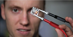
At DTU Nanotech, a method for accurately monitoring the decoupling of graphene from copper catalysts during oxidation in water has been developed. The method is based on the so-called Raman spectroscopy, a standard characterization tool in the graphene community. Patrick Whelan explains that “using the new method, it is possible for us to measure if the graphene is fully decoupled from the copper catalysts and thus we have been able to transfer graphene by mechanical peeling from 12inch diameter copper thin films”. (See figure 1).
Figure 1: Transferring graphene from a 12 inch copper substrate using a supporting polymer film
Patrick’s research is part of two larger research projects involving a number of industrial as well as academic partners. One of these partners is Cambridge University where Patrick had an external stay. The collaboration in Cambridge resulted in the development of another new transfer method, where the graphene is released from the copper substrate by intercalation of basic solution between graphene and copper. The electrical properties of graphene transferred by this method are superior when compared to standard transfer techniques.
Graphene-based OLEDs
The new transfer technique developed at Cambridge University has made it possible to fabricate OLEDs where graphene is used as replacement for indium tin oxide (ITO) as transparent conducting electrode (see figure 2). These OLEDs are made in collaboration with Fraunhofer COMEDD (Dresden, Germany) which is a research project partner specialized in organic electronics. Today, ITO is the material which is most frequently used as transparent conducting electrode. However, the researchers are able to achieve higher power efficiencies from OLEDs built on a single layer of graphene compared to ITO-based OLEDs.
Figure 2: OLED with graphene as transparent top electrode
Patrick explains that “the next step is to focus on increasing the conductivity of the transferred graphene layers and thus the power efficiency of the OLEDs. We see two possible routes for this: We can stack multiple graphene layers and/or we can dope the graphene chemically, that is we can introduce impurities that affect the electrical properties. This should enable graphene to be even more competitive with ITO”.
At DTU Fotonik the conductivity of the graphene can be mapped by the so-called THz spectroscopy, a fast and non-contact measuring technique, which makes it easy to test the influence of different doping methods.
“In the future, we hope that graphene can become the standard material as electrode for flexible electronics, which for instance can be used to make bendable screens. The markets for wearable electronics and e-textiles are expected to grow over the coming years and it is possible that graphene could also play a role in such products due to its flexibility, conductivity, and light weight”, says Patrick.
The research was carried out in the DA-GATE (Danish Alliance for Graphene Applications, Technology and Engineering) project, funded by Innovation Fund Denmark, and the GLADIATOR (Graphene Layers: Production, Characterization and Integration) project funded by EU FP7.
Share on:


Testimonial
"The I-Connect007 team is outstanding—kind, responsive, and a true marketing partner. Their design team created fresh, eye-catching ads, and their editorial support polished our content to let our brand shine. Thank you all! "
Sweeney Ng - CEE PCBSuggested Items
Trouble in Your Tank: Implementing Direct Metallization in Advanced Substrate Packaging
09/15/2025 | Michael Carano -- Column: Trouble in Your TankDirect metallization systems based on conductive graphite are gaining popularity throughout the world. The environmental and productivity gains achievable with this process are outstanding. Direct metallization reduces the costs of compliance, waste treatment, and legal issues related to chemical exposure. A graphite-based direct plate system has been devised to address these needs.
Closing the Loop on PCB Etching Waste
09/09/2025 | Shawn Stone, IECAs the PCB industry continues its push toward greener, more cost-efficient operations, Sigma Engineering’s Mecer System offers a comprehensive solution to two of the industry’s most persistent pain points: etchant consumption and rinse water waste. Designed as a modular, fully automated platform, the Mecer System regenerates spent copper etchants—both alkaline and acidic—and simultaneously recycles rinse water, transforming a traditionally linear chemical process into a closed-loop system.
Driving Innovation: Depth Routing Processes—Achieving Unparalleled Precision in Complex PCBs
09/08/2025 | Kurt Palmer -- Column: Driving InnovationIn PCB manufacturing, the demand for increasingly complex and miniaturized designs continually pushes the boundaries of traditional fabrication methods, including depth routing. Success in these applications demands not only on robust machinery but also sophisticated control functions. PCB manufacturers rely on advanced machine features and process methodologies to meet their precise depth routing goals. Here, I’ll explore some crucial functions that empower manufacturers to master complex depth routing challenges.
Trouble in Your Tank: Minimizing Small-via Defects for High-reliability PCBs
08/27/2025 | Michael Carano -- Column: Trouble in Your TankTo quote the comedian Stephen Wright, “If at first you don’t succeed, then skydiving is not for you.” That can be the battle cry when you find that only small-diameter vias are exhibiting voids. Why are small holes more prone to voids than larger vias when processed through electroless copper? There are several reasons.
The Government Circuit: Navigating New Trade Headwinds and New Partnerships
08/25/2025 | Chris Mitchell -- Column: The Government CircuitAs global trade winds continue to howl, the electronics manufacturing industry finds itself at a critical juncture. After months of warnings, the U.S. Government has implemented a broad array of tariff increases, with fresh duties hitting copper-based products, semiconductors, and imports from many nations. On the positive side, tentative trade agreements with Europe, China, Japan, and other nations are providing at least some clarity and counterbalance.