


 The Marketing Minute: Cracking the Code of Technical Marketing
 Trouble in Your Tank: Implementing Direct Metallization in Advanced Substrate Packaging


Sandwiched Between Superconductors, Graphene Adopts Exotic Electronic States
May 5, 2017 | MITEstimated reading time: 4 minutes
In normal conductive materials such as silver and copper, electric current flows with varying degrees of resistance, in the form of individual electrons that ping-pong off defects, dissipating energy as they go. Superconductors, by contrast, are so named for their remarkable ability to conduct electricity without resistance, by means of electrons that pair up and move through a material as one, generating no friction.
Now MIT physicists have found that a flake of graphene, when brought in close proximity with two superconducting materials, can inherit some of those materials’ superconducting qualities. As graphene is sandwiched between superconductors, its electronic state changes dramatically, even at its center.
The researchers found that graphene’s electrons, formerly behaving as individual, scattering particles, instead pair up in “Andreev states” — a fundamental electronic configuration that allows a conventional, nonsuperconducting material to carry a “supercurrent,” an electric current that flows without dissipating energy.
Their findings, published this week in Nature Physics, are the first investigation of Andreev states due to superconductivity’s “proximity effect” in a two-dimensional material such as graphene.
Down the road, the researchers’ graphene platform may be used to explore exotic particles, such as Majorana fermions, which are thought to arise from Andreev states and may be key particles for building powerful, error-proof quantum computers.
“There is a huge effort in the condensed physics community to look for exotic quantum electronic states,” says lead author Landry Bretheau, a postdoc in MIT’s Department of Physics. “In particular, new particles called Majorana fermions are predicted to emerge in graphene that is connected to superconducting electrodes and exposed to large magnetic fields. Our experiment is promising, as we are unifying some of these ingredients.”
Landry’s MIT co-authors are postdoc Joel I-Jan Wang, visiting student Riccardo Pisoni, and associate professor of physics Pablo Jarillo-Herrero, along with Kenji Watanabe and Takashi Taniguchi of the National Institute for Materials Science, in Japan.
The superconducting proximity effect
In 1962, the British physicist Brian David Josephson predicted that two superconductors sandwiching a nonsuperconducting layer between them could sustain a supercurrent of electron pairs, without any external voltage.
As a whole, the supercurrent associated with the Josephson effect has been measured in numerous experiments. But Andreev states — considered the microscopic building blocks of a supercurrent — have been observed only in a handful of systems, such as silver wires, and never in a two-dimensional material.
Bretheau, Wang, and Jarillo-Herrero tackled this issue by using graphene — an ultrathin sheet of interlinked carbon atoms — as the nonsuperconducting material. Graphene, as Bretheau explains, is an extremely “clean” system, exhibiting very little scattering of electrons. Graphene’s extended, atomic configuration also enables scientists to measure graphene’s electronic Andreev states as the material comes in contact with superconductors. Scientists can also control the density of electrons in graphene and investigate how it affects the superconducting proximity effect.
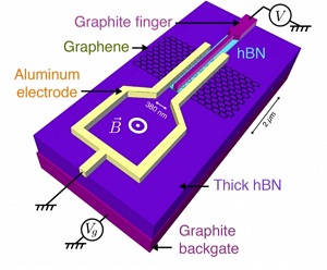
The researchers exfoliated a very thin flake of graphene, just a few hundred nanometers wide, from a larger chunk of graphite, and placed the flake on a small platform made from a crystal of boron nitride overlaying a sheet of graphite. On either end of the graphene flake, they placed an electrode made from aluminum, which behaves as a superconductor at low temperatures. They then placed the entire structure in a dilution refrigerator and lowered the temperature to 20 millikelvin — well within aluminum’s superconducting range.
“Frustrated” states
In their experiments, the researchers varied the magnitude of the supercurrent flowing between the superconductors by applying a changing magnetic field to the entire structure. They also applied an external voltage directly to graphene, to vary the number of electrons in the material.
Under these changing conditions, the team measured the graphene’s density of electronic states while the flake was in contact with both aluminum superconductors. Using tunneling spectroscopy, a common technique that measures the density of electronic states in a conductive sample, the researchers were able to probe the graphene’s central region to see whether the superconductors had any effect, even in areas where they weren’t physically touching the graphene.
The measurements indicated that graphene’s electrons, which normally act as individual particles, were pairing up, though in “frustrated” configurations, with energies dependent on magnetic field.
“Electrons in a superconductor dance harmoniously in pairs, like a ballet, but the choreography in the left and right superconductors can be different,” Bretheau says. “Pairs in the central graphene are frustrated as they try to satisfy both ways of dancing. These frustrated pairs are what physicists know as Andreev states; they are carrying the supercurrent.”
Bretheau and Wang found Andreev states vary their energy in response to a changing magnetic field. Andreev states are more pronounced when graphene has a higher density of electrons and there is a stronger supercurrent running between electrodes.
“[The superconductors] are actually giving graphene some superconducting qualities,” Bretheau says. “We found these electrons can be dramatically affected by superconductors.”
While the researchers carried out their experiments under low magnetic fields, they say their platform may be a starting point for exploring the more exotic Majorana fermions that should appear under high magnetic fields.
“There are proposals for how to use Majorana fermions to build powerful quantum computers,” Bretheau says. “These particles could be the elementary brick of topological quantum computers, with very strong protection against errors. Our work is an initial step in this direction.”
This work was supported, in part, by the U.S. Department of Energy and the Gordon and Betty Moore Foundation.
Share on:


Testimonial
"Advertising in PCB007 Magazine has been a great way to showcase our bare board testers to the right audience. The I-Connect007 team makes the process smooth and professional. We’re proud to be featured in such a trusted publication."
Klaus Koziol - atgSuggested Items
Trouble in Your Tank: Implementing Direct Metallization in Advanced Substrate Packaging
09/15/2025 | Michael Carano -- Column: Trouble in Your TankDirect metallization systems based on conductive graphite are gaining popularity throughout the world. The environmental and productivity gains achievable with this process are outstanding. Direct metallization reduces the costs of compliance, waste treatment, and legal issues related to chemical exposure. A graphite-based direct plate system has been devised to address these needs.
Closing the Loop on PCB Etching Waste
09/09/2025 | Shawn Stone, IECAs the PCB industry continues its push toward greener, more cost-efficient operations, Sigma Engineering’s Mecer System offers a comprehensive solution to two of the industry’s most persistent pain points: etchant consumption and rinse water waste. Designed as a modular, fully automated platform, the Mecer System regenerates spent copper etchants—both alkaline and acidic—and simultaneously recycles rinse water, transforming a traditionally linear chemical process into a closed-loop system.
Driving Innovation: Depth Routing Processes—Achieving Unparalleled Precision in Complex PCBs
09/08/2025 | Kurt Palmer -- Column: Driving InnovationIn PCB manufacturing, the demand for increasingly complex and miniaturized designs continually pushes the boundaries of traditional fabrication methods, including depth routing. Success in these applications demands not only on robust machinery but also sophisticated control functions. PCB manufacturers rely on advanced machine features and process methodologies to meet their precise depth routing goals. Here, I’ll explore some crucial functions that empower manufacturers to master complex depth routing challenges.
Trouble in Your Tank: Minimizing Small-via Defects for High-reliability PCBs
08/27/2025 | Michael Carano -- Column: Trouble in Your TankTo quote the comedian Stephen Wright, “If at first you don’t succeed, then skydiving is not for you.” That can be the battle cry when you find that only small-diameter vias are exhibiting voids. Why are small holes more prone to voids than larger vias when processed through electroless copper? There are several reasons.
The Government Circuit: Navigating New Trade Headwinds and New Partnerships
08/25/2025 | Chris Mitchell -- Column: The Government CircuitAs global trade winds continue to howl, the electronics manufacturing industry finds itself at a critical juncture. After months of warnings, the U.S. Government has implemented a broad array of tariff increases, with fresh duties hitting copper-based products, semiconductors, and imports from many nations. On the positive side, tentative trade agreements with Europe, China, Japan, and other nations are providing at least some clarity and counterbalance.