


 The Marketing Minute: Cracking the Code of Technical Marketing
 Trouble in Your Tank: Implementing Direct Metallization in Advanced Substrate Packaging


Scientists Print Nanoscale Imaging Probe onto Tip of Optical Fiber
May 10, 2017 | Berkeley LabEstimated reading time: 4 minutes
Combining speed with incredible precision, a team of researchers has developed a way to print a nanoscale imaging probe onto the tip of a glass fiber as thin as a human hair, accelerating the production of the promising new device from several per month to several per day.
The high-throughput fabrication technique opens the door for the widespread adoption of this and other nano-optical structures, which squeeze and manipulate light in ways that are unachievable by conventional optics. Nano-optics have the potential to be used for imaging, sensing, and spectroscopy, and could help scientists improve solar cells, design better drugs, and make faster semiconductors. A big obstacle to the technology’s commercial use, however, is its time-consuming production process.
The new fabrication method, called fiber nanoimprinting, could unplug this bottleneck. It was developed by scientists at the Molecular Foundry, located at the Department of Energy’s Lawrence Berkeley National Laboratory (Berkeley Lab), in partnership with scientists from Hayward, California-based aBeam Technologies. Their research is reported online May 10 in the journal Scientific Reports.
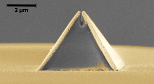
Their work builds on the Campanile probe, which was developed by Molecular Foundry scientists four years ago. Its tapered, four-sided shape resembles the top of the Campanile clock tower on UC Berkeley’s campus. The probe is mounted at the end of an optical fiber, and focuses an intense beam of light onto a much smaller spot than is possible with current optics. This enables spectroscopic imaging at a resolution 100 times greater than conventional spectroscopy, which only maps the average chemical composition of a material.
In contrast, the Campanile probe can image the molecule-by-molecule makeup of nanoparticles and other materials. Scientists can use it to examine a nanowire for minute defects, for example, leading to new ways to improve nanowires for use in more efficient solar cells.
But fabricating Campanile probes has been part science and part art. The same applies to other nano-optical devices, such as microscopic lenses and beam splitters, which split one light beam into several. These devices require milling a 3-D shape with sub-100-nanometer scale features on the tip of a wispy fiber, which is much trickier than fabricating a nanostructure on a flat surface such as a wafer.
“When we first made the Campanile probe, we sculpted it with an ion beam like Michelangelo. It took about a month,” says Stefano Cabrini, director of the Nanofabrication Facility at the Molecular Foundry. “That pace is OK for research applications, but the lack of a mass-fabrication method has inhibited the wider use of nano-optical devices.”
That’s where fiber nanoimprinting come in. Its first step is the most time consuming: Scientists create a mold with the precise dimensions of the nano-optical device they want to print. For the Campanile probe, this means a mold of the probe’s nanoscale features, including the four sides and the light-emitting 70-nanometer-wide gap at the pyramid’s top.
“This mold can take a few weeks to make, but we only need one, and then we can start printing,” explains Keiko Munechika of aBeam Technologies, which partnered with the Molecular Foundry to develop the fabrication process as part of the Department of Energy’s Small Business Technology Transfer program. Several other aBeam Technologies scientists contributed to this work, including Alexander Koshelev. The company is now commercializing various fiber-based nano-optical devices (see additional information).
After the mold is created, it’s off to the races. The mold is filled with a special resin and then positioned atop an optical fiber. Infrared light is sent through the fiber, which enables the scientists to measure the exact alignment of the mold in relation to the fiber. If everything checks out, UV light is sent through the fiber, which hardens the resin. A final metallization step coats the sides of the probe with gold layers. The result is a quickly printed—not meticulously sculpted—Campanile probe.
“We can do this over and over and make a probe every few minutes,” says Munechika.
There are several advantages to the faster production pace. Campanile probes are fragile, and now it’s possible to give researchers a batch in case one breaks. Plus it’s easier to optimize nano-optical devices if scientists are able to provide feedback on a device’s performance, and an improved batch is quickly developed for further testing. The fabrication technique can also be applied to any nano-optical device, and has so far been used to create Fresnel lenses and beam splitters in addition to the Campanile probe.
“Instead of sculpting a one-of-a-kind device like Michelangelo, we now take the original masterpiece, make an imprint of it, and create many replicas in quick succession,” says Cabrini. “It’s a new capability the Molecular Foundry can provide to the science community.”
The Molecular Foundry is a DOE Office of Science User Facility. The research was primarily supported by the Department of Energy’s Office of Science.
About Lawrence Berkeley National Laboratory
Lawrence Berkeley National Laboratory addresses the world’s most urgent scientific challenges by advancing sustainable energy, protecting human health, creating new materials, and revealing the origin and fate of the universe. Founded in 1931, Berkeley Lab’s scientific expertise has been recognized with 13 Nobel Prizes. The University of California manages Berkeley Lab for the U.S. Department of Energy’s Office of Science.
About DOE
DOE’s Office of Science is the single largest supporter of basic research in the physical sciences in the United States, and is working to address some of the most pressing challenges of our time.
Share on:


Testimonial
"Our marketing partnership with I-Connect007 is already delivering. Just a day after our press release went live, we received a direct inquiry about our updated products!"
Rachael Temple - AlltematedSuggested Items
MEMS & Imaging Sensors Summit to Spotlight Sensing Revolution for Europe’s Leadership
09/11/2025 | SEMIIndustry experts will gather November 19-20 at the SEMI MEMS & Imaging Sensors Summit 2025 to explore the latest breakthroughs in AI-driven MEMS and imaging optimization, AR/VR technologies, and advanced sensor solutions for critical defence applications.
Direct Imaging System Market Size to Hit $4.30B by 2032, Driven by Increasing Demand for High-Precision PCB Manufacturing
09/11/2025 | Globe NewswireAccording to the SNS Insider, “The Direct Imaging System Market size was valued at $2.21 Billion in 2024 and is projected to reach $4.30 Billion by 2032, growing at a CAGR of 8.68% during 2025-2032.”
I-Connect007’s Editor’s Choice: Five Must-Reads for the Week
07/04/2025 | Marcy LaRont, I-Connect007For our industry, we have seen several bullish market announcements over the past few weeks, including one this week by IDC on the massive growth in the global server market. We’re also closely watching global trade and nearshoring. One good example of successful nearshoring is Rehm Thermal Systems, which celebrates its 10th anniversary in Mexico and the official opening of its new building in Guadalajara.
Driving Innovation: Direct Imaging vs. Conventional Exposure
07/01/2025 | Simon Khesin -- Column: Driving InnovationMy first camera used Kodak film. I even experimented with developing photos in the bathroom, though I usually dropped the film off at a Kodak center and received the prints two weeks later, only to discover that some images were out of focus or poorly framed. Today, every smartphone contains a high-quality camera capable of producing stunning images instantly.
United Electronics Corporation Advances Manufacturing Capabilities with Schmoll MDI-ST Imaging Equipment
06/24/2025 | United Electronics CorporationUnited Electronics Corporation has successfully installed the advanced Schmoll MDI-ST (XL) imaging equipment at their advanced printed circuit board facility. This significant technology investment represents a continued commitment to delivering superior products and maintaining their position as an industry leader in precision PCB manufacturing.