


 The Marketing Minute: Cracking the Code of Technical Marketing
 Trouble in Your Tank: Implementing Direct Metallization in Advanced Substrate Packaging


Laying the Foundations for Hybrid Silicon Lasers
June 16, 2017 | A*STAREstimated reading time: 2 minutes
Producing semiconductor lasers on a silicon wafer is a long-held goal for the electronics industry, but their fabrication has proved challenging. Now, researchers at A*STAR have developed an innovative way to manufacture them that is cheap, simple and scalable.
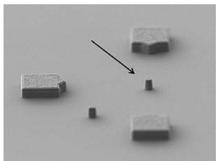
Oblique angle scanning electron microscopy image of a 500 nanometer diameter microdisk.
Hybrid silicon lasers combine the light-emitting properties of group III–V semiconductors, like gallium arsenide and indium phosphide, with the maturity of silicon manufacturing techniques. These lasers are attracting considerable attention as they promise inexpensive, mass-producible optical devices that can integrate with photonic and microelectronic elements on a single silicon chip. They have potential in a wide range of applications, from short-distance data communication to high-speed, long-distance optical transmission.
In the current production process, however, lasers are fabricated on separate III–V semiconductor wafers before being individually aligned to each silicon device — a time-consuming, costly process that limits the number of lasers that can be placed on a chip.
To overcome these limitations, Doris Keh-Ting Ng and her colleagues from the A*STAR Data Storage Institute have developed an innovative method for producing a hybrid III–V semiconductor and silicon-on-insulator (SOI) optical microcavity. This greatly reduces the complexity of the fabrication process and results in a more compact device.
“It’s very challenging to etch the entire cavity,” says Ng. “Currently, there is no single etch recipe and mask that allows the whole microcavity to be etched, and so we decided to develop a new approach.”
By first attaching a thin film of III–V semiconductor to a silicon oxide (SiO2) wafer using a SOI interlayer thermal bonding process, they produced a strong bond that also removes the need for strong oxidizing agents, such as Piranha solution or hydrofluoric acid.
And by using a dual hard-mask technique to etch the microcavity that confined etching to the intended layer, they eliminated the requirement to use multiple overlay lithography and etching cycles — a challenging procedure.
“Our approach cuts down the number of fabrication steps, reduces the use of hazardous chemicals, and requires only one lithography step to complete the process,” explains Ng.
The work presents, for the first time, a new heterocore configuration and integrated fabrication process that combines low-temperature SiO2 interlayer bonding with dual hard-mask, single lithography patterning.
“The process not only makes it possible to produce heterocore devices, it also greatly reduces the challenges of fabricating them, and could serve as an alternative hybrid microcavity for use by the research community,” says Ng.
Share on:


Testimonial
"The I-Connect007 team is outstanding—kind, responsive, and a true marketing partner. Their design team created fresh, eye-catching ads, and their editorial support polished our content to let our brand shine. Thank you all! "
Sweeney Ng - CEE PCBSuggested Items
Alternative Manufacturing, Inc. (AMI) Announces Commitment to Excellence in Industrial, Defense, Aerospace, Renewables, and Robotics Markets
09/16/2025 | Alternative Manufacturing, Inc.Alternative Manufacturing, Inc. (AMI), a 100% employee-owned contract manufacturer, proudly reaffirms its leadership in the electronics manufacturing services (EMS) industry with a continued commitment to delivering high-quality PCBAs and box builds across the industrial, defense, aerospace, renewable energy, and robotics markets.
Sustainability and Selective Soldering
09/15/2025 | Dr. Samuel J. McMaster, Pillarhouse InternationalSustainability is more than just a buzzword for the electronics industry; it’s a key goal for all manufacturing processes. This is more than a box-ticking exercise or simply doing a small part for environmentally friendly processes. Moving toward sustainable solutions drives innovation and operational efficiency.
Trouble in Your Tank: Implementing Direct Metallization in Advanced Substrate Packaging
09/15/2025 | Michael Carano -- Column: Trouble in Your TankDirect metallization systems based on conductive graphite are gaining popularity throughout the world. The environmental and productivity gains achievable with this process are outstanding. Direct metallization reduces the costs of compliance, waste treatment, and legal issues related to chemical exposure. A graphite-based direct plate system has been devised to address these needs.
EV Group Achieves Breakthrough in Hybrid Bonding Overlay Control for Chiplet Integration
09/12/2025 | EV GroupEV Group (EVG), a leading provider of innovative process solutions and expertise serving leading-edge and future semiconductor designs and chip integration schemes, today unveiled the EVG®40 D2W—the first dedicated die-to-wafer overlay metrology platform to deliver 100 percent die overlay measurement on 300-mm wafers at high precision and speeds needed for production environments. With up to 15X higher throughput than EVG’s industry benchmark EVG®40 NT2 system designed for hybrid wafer bonding metrology, the new EVG40 D2W enables chipmakers to verify die placement accuracy and take rapid corrective action, improving process control and yield in high-volume manufacturing (HVM).
Integrating Uniplate PLBCu6 With the Digital Factory Suite
09/12/2025 | Giovanni Obino and Andreas Schatz, MKS' AtotechPrinted circuit board manufacturing is rapidly changing, driven by miniaturization, stringent reliability requirements, and growing pressure for sustainable production. Meeting these challenges requires more than incremental improvements; it demands a combination of precise equipment and real-time process intelligence. The pairing of Uniplate® PLBCu6 with the Digital Factory Suite (DFS) demonstrates how hardware and software can work together to create more responsive, resource-efficient manufacturing.