


 The Marketing Minute: Cracking the Code of Technical Marketing
 Trouble in Your Tank: Implementing Direct Metallization in Advanced Substrate Packaging


Making Wires of Polymer Chains
June 16, 2017 | A*STAREstimated reading time: 2 minutes
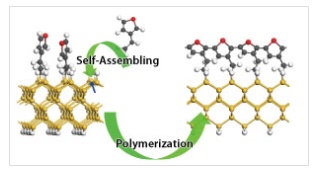
Consumer demand continually pushes the electronics industry to design smaller devices. Now researchers at A*STAR have used a theoretical model to assess the potential of electric wires made from polymer chains that could help with miniaturization.
As conventional silicon-integrated circuits reach their lower size limit, new concepts are required such as molecular electronics — the use of electronic components comprised of molecular building blocks. Shuo-Wang Yang at A*STAR Institute of High Performance Computing together with his colleagues and collaborators, are using computer modeling to design electric wires made of polymer chains.
“It has been a long-standing goal to make conductive molecular wires on traditional semiconductor or insulator substrates to satisfy the ongoing demand miniaturization in electronic devices,” explains Yang.
Progress has been delayed in identifying molecules that both conduct electricity and bind to substrates. “Structures with functional groups that facilitate strong surface adsorption typically exhibit poor electrical conductivity, because charge carriers tend to localize at these groups,” he adds.
Yang’s team applied density functional theory to a two-step approach for synthesizing linear polymer chains on a silicon surface1,2. “This theory is the best simulation method for uncovering the mechanism behind chemical reactions at atomic and electronic levels. It can be used to predict the reaction pathways to guide researchers,” says Yang.
The first step is the self-assembled growth of single monomers on to the silicon surface. Yang’s team studied several potential monomers including, most recently, a thiophene substituted alkene1 and a symmetrical benzene ring with three alkynes attached2. The second step is the polymerization of the tethered monomers by adding a radical to the system.
According to the calculations, these tethered polymers are semiconductors in their natural state. “We introduced some holes, such as atomic defects, to the wires to shift the Fermi levels and make them conductive,” Yang explains.
The team then studied the electron band structures of each component before and after tethering and polymerization; finding little charge transfer between the molecular wires and the silicon surfaces. “The surface-grafted polymers and underlying substrates seem independent of each other, which is an ideal model of a conductive molecular wire on a traditional semiconductor substrate,” says Yang.
“Our finding provides a theoretical guide to fabricating ideal molecular wires on traditional semiconducting surfaces,” he adds. The team is plans to extend their work to study 2D analogs of these 1D polymer chains that could work as a metallic layer in molecular electronic devices.
Share on:


Testimonial
"The I-Connect007 team is outstanding—kind, responsive, and a true marketing partner. Their design team created fresh, eye-catching ads, and their editorial support polished our content to let our brand shine. Thank you all! "
Sweeney Ng - CEE PCBSuggested Items
Driving Innovation: Depth Routing Processes—Achieving Unparalleled Precision in Complex PCBs
09/08/2025 | Kurt Palmer -- Column: Driving InnovationIn PCB manufacturing, the demand for increasingly complex and miniaturized designs continually pushes the boundaries of traditional fabrication methods, including depth routing. Success in these applications demands not only on robust machinery but also sophisticated control functions. PCB manufacturers rely on advanced machine features and process methodologies to meet their precise depth routing goals. Here, I’ll explore some crucial functions that empower manufacturers to master complex depth routing challenges.
Polar Instruments Announces Additive Transmission Line Support for Si9000e
08/20/2025 | Polar InstrumentsTransmission lines embedded into the PCB surface are a feature of UHDI constructions. The 2025 fall release of Polar's Si9000e PCB impedance & insertion loss transmission line field solver incorporates eight new single ended, differential and coplanar transmission line structures.
Henniker Plasma Launches Stratus Turnkey Plasma Manufacturing Cell
08/13/2025 | Henniker PlasmaHenniker Plasma, a leading manufacturer of plasma treatment systems, proudly announces the launch of its Stratus Plasma Manufacturing Cell range — a fully integrated, turnkey solution that combines advanced atmospheric plasma surface treatment with robotic automation.
Trouble in Your Tank: Metallizing Flexible Circuit Materials—Mitigating Deposit Stress
08/04/2025 | Michael Carano -- Column: Trouble in Your TankMetallizing materials, such as polyimide used for flexible circuitry and high-reliability multilayer printed wiring boards, provide a significant challenge for process engineers. Conventional electroless copper systems often require pre-treatments with hazardous chemicals or have a small process window to achieve uniform coverage without blistering. It all boils down to enhancing the adhesion of the thin film of electroless copper to these smooth surfaces.
Designers Notebook: Basic PCB Planning Criteria—Establishing Design Constraints
07/22/2025 | Vern Solberg -- Column: Designer's NotebookPrinted circuit board development flows more smoothly when all critical issues are predefined and understood from the start. As a basic planning strategy, the designer must first consider the product performance criteria, then determine the specific industry standards or specifications that the product must meet. Planning also includes a review of all significant issues that may affect the product’s manufacture, performance, reliability, overall quality, and safety.