


 The Marketing Minute: Cracking the Code of Technical Marketing
 Trouble in Your Tank: Implementing Direct Metallization in Advanced Substrate Packaging


New Research Finds a Missing Piece to High-Temperature Superconductor Mystery
June 20, 2017 | SLAC National Accelerator LaboratoryEstimated reading time: 4 minutes
An international team led by scientists from the Department of Energy’s SLAC National Accelerator Laboratory and Stanford University has detected new features in the electronic behavior of a copper oxide material that may help explain why it becomes a perfect electrical conductor – a superconductor – at relatively high temperatures.
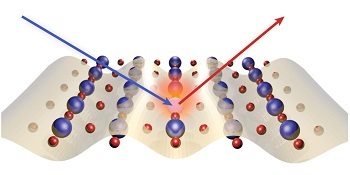
This sketch shows how resonant inelastic X-ray scattering (RIXS) helps scientists understand the electronic behavior of copper oxide materials. An X-ray photon aimed at the sample (blue arrow) is absorbed by a copper atom, which then emits a new, lower-energy photon (red arrow) as it relaxes. The amount of momentum transferred and energy lost in this process can induce changes in the charge density waves thought to be important in high-temperature superconductivity. (Wei-Sheng/SLAC National Accelerator Laboratory)
Using an ultrahigh-resolution X-ray instrument in France, the researchers for the first time saw dynamic behaviors in the material’s charge density wave (CDW) – a pattern of electrons that resembles a standing wave – that lend support to the idea that these waves may play a role in high-temperature superconductivity.
Data taken at low (20 kelvins) and high (240 kelvins) temperatures showed that as the temperature increased, the CDW became more aligned with the material’s atomic structure. Remarkably, at the lower temperature, the CDW also induced an unusual increase in the intensity of the oxide’s atomic lattice vibrations, indicating that the dynamic CDW behaviors can propagate through the lattice.
“Previous research has shown that when the CDW is static, it competes with and diminishes superconductivity,” said co-author Wei-Sheng Lee, a SLAC staff scientist and investigator with the Stanford Institute for Materials and Energy Sciences (SIMES), which led the study published June 12 in Nature Physics. “If, on the other hand, the CDW is not static but fluctuating, theory tells us they may actually help form superconductivity.”
A Decades-long Search for an Explanation
The new result is the latest in a decades-long search by researchers worldwide for the factors that enable certain materials to become superconducting at relatively high temperatures.
Since the 1950s, scientists have known how certain metals and simple alloys become superconducting when chilled to within a few degrees of absolute zero: Their electrons pair up and ride waves of atomic vibrations that act like a virtual glue to hold the pairs together. Above a certain temperature, however, the glue fails as thermal vibrations increase, the electron pairs split up and superconductivity disappears.
In 1986, complex copper oxide materials were found to become superconducting at much higher – although still quite cold – temperatures. This discovery was so unexpected it caused a worldwide scientific sensation. By understanding and optimizing how these materials work, researchers hope to develop superconductors that work at room temperature and above.
At first, the most likely glue holding superconducting electron pairs together at higher temperatures seemed to be strong magnetic excitations created by interactions between electron spins. But in 2014, a theoretical simulation and experiments led by SIMES researchers concluded that these high-energy magnetic interactions are not the sole factor in copper oxide’s high-temperature superconductivity. An unanticipated CDW also appeared to be important.
The latest results continue the SIMES collaboration between experiment and theory. Building upon previous theories of how electron interactions with lattice vibrations can be probed with resonant inelastic X-ray scattering, or RIXS, the signature of CDW dynamics was finally identified, providing additional support for the CDW’s role in determining the electronic structure in superconducting copper oxides.
The Essential New Tool: RIXS
The new results are enabled by the development of more capable instruments employing RIXS. Now available at ultrahigh resolution at the European Synchrotron Radiation Facility (ESRF) in France, where the team performed this experiment, RIXS will also be an important feature of SLAC’s upgraded Linac Coherent Light Source X-ray free-electron laser, LCLS-II. The combination of ultrahigh energy resolution and a high pulse repetition rate at LCLS-II will enable researchers to see more detailed CDW fluctuations and perform experiments aimed at revealing additional details of its behavior and links to high-temperature superconductivity. Most importantly, researchers at LCLS-II will be able to use ultrafast light-matter interactions to control CDW fluctuations and then take femtosecond-timescale snapshots of them.
RIXS involves illuminating a sample with X-rays that have just enough energy to excite some electrons deep inside the target atoms to jump up into a specific higher orbit. When the electrons relax back down into their previous positions, a tiny fraction of them emit X-rays that carry valuable atomic-scale information about the material's electronic and magnetic configuration that is thought to be important in high-temperature superconductivity.
“To date, no other technique has seen evidence of propagating CDW dynamics,” Lee said.
RIXS was first demonstrated in the mid-1970s, but it could not obtain useful information to address key problems until 2007, when Giacomo Ghiringhelli, Lucio Braicovich at Milan Polytechnic in Italy and colleagues at Swiss Light Source made a fundamental change that improved its energy resolution to a level where significant details became visible – technically speaking to about 120 milli-electronvolts (meV) at the relevant X-ray wavelength, which is called a copper L edge. The new RIXS instrument at ESRF is three times better, routinely attaining an energy resolution down to 40 meV. Since 2014, the Milan group has collaborated with SLAC and Stanford scientists in their RIXS research.
“The new ultrahigh resolution RIXS makes a huge difference,” Lee said. “It can show us previously invisible details.”
Other researchers involved in this result were from Milan Polytechnic, European Synchrotron Radiation Facility, Japan’s National Institute of Advanced Industrial Science and Technology and Italy’s National Research Council Institute for Superconductors, Oxides and Other Innovative Materials and Devices (CNR-SPIN). Funding for this research came from the DOE Office of Science.
Share on:


Testimonial
"We’re proud to call I-Connect007 a trusted partner. Their innovative approach and industry insight made our podcast collaboration a success by connecting us with the right audience and delivering real results."
Julia McCaffrey - NCAB GroupSuggested Items
Trouble in Your Tank: Implementing Direct Metallization in Advanced Substrate Packaging
09/15/2025 | Michael Carano -- Column: Trouble in Your TankDirect metallization systems based on conductive graphite are gaining popularity throughout the world. The environmental and productivity gains achievable with this process are outstanding. Direct metallization reduces the costs of compliance, waste treatment, and legal issues related to chemical exposure. A graphite-based direct plate system has been devised to address these needs.
Closing the Loop on PCB Etching Waste
09/09/2025 | Shawn Stone, IECAs the PCB industry continues its push toward greener, more cost-efficient operations, Sigma Engineering’s Mecer System offers a comprehensive solution to two of the industry’s most persistent pain points: etchant consumption and rinse water waste. Designed as a modular, fully automated platform, the Mecer System regenerates spent copper etchants—both alkaline and acidic—and simultaneously recycles rinse water, transforming a traditionally linear chemical process into a closed-loop system.
Driving Innovation: Depth Routing Processes—Achieving Unparalleled Precision in Complex PCBs
09/08/2025 | Kurt Palmer -- Column: Driving InnovationIn PCB manufacturing, the demand for increasingly complex and miniaturized designs continually pushes the boundaries of traditional fabrication methods, including depth routing. Success in these applications demands not only on robust machinery but also sophisticated control functions. PCB manufacturers rely on advanced machine features and process methodologies to meet their precise depth routing goals. Here, I’ll explore some crucial functions that empower manufacturers to master complex depth routing challenges.
Trouble in Your Tank: Minimizing Small-via Defects for High-reliability PCBs
08/27/2025 | Michael Carano -- Column: Trouble in Your TankTo quote the comedian Stephen Wright, “If at first you don’t succeed, then skydiving is not for you.” That can be the battle cry when you find that only small-diameter vias are exhibiting voids. Why are small holes more prone to voids than larger vias when processed through electroless copper? There are several reasons.
The Government Circuit: Navigating New Trade Headwinds and New Partnerships
08/25/2025 | Chris Mitchell -- Column: The Government CircuitAs global trade winds continue to howl, the electronics manufacturing industry finds itself at a critical juncture. After months of warnings, the U.S. Government has implemented a broad array of tariff increases, with fresh duties hitting copper-based products, semiconductors, and imports from many nations. On the positive side, tentative trade agreements with Europe, China, Japan, and other nations are providing at least some clarity and counterbalance.